In this part, a tutorial on the FPGA implementation of digital systems is discussed. A simplified version of FPGA based design flow is given in the following diagram.

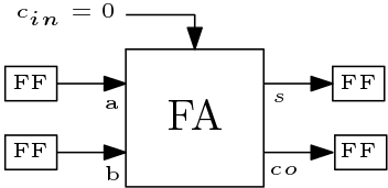
Lets consider an example to illustrate the FPGA implementation procedure. The circuit shown in Fig. 2 is considered as a test circuit.
Design Entry
There are different techniques for design entry.
- Schematic based,
- Hardware Description Language (VHDL, VERILOG)
- Combination of both.
Selection of a method depends on the design and the designer. If the designer wants to deal more with hardware, then Schematic entry is a better choice. When the design is complex or the designer wants to realize the design in an algorithmic way then HDL is the better choice. Language based entry is faster but lag in performance and density. HDLs represent a level of abstraction that can isolate the designers from the details of the hardware implementation. Schematic based entry gives designers much more visibility into the hardware. Another method but rarely used is state machines. It is the better choice for the designers who think the design as a series of states. But the tools for state machine entry are limited. Design entry using the structural style is combination of both schematic and HDL. We preferred design entry by Verilog HDL in structural style to understand hardware details without much complexity.
Synthesis
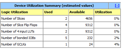
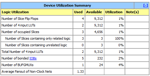
Synthesis is the process which translates VHDL or Verilog code into a device netlist format i.e. a complete circuit with logical elements (gates, flip flops, etc.) for the design. If the design contains more than one sub designs, ex. to implement a processor, we need a CPU as one design element and RAM as another and so on, and then the synthesis process generates netlist for each design element. Synthesis process will check code syntax and analyze the hierarchy of the design which ensures that the design is optimized for the design architecture, the designer has selected. The resulting netlist(s) is saved to an NGC (Native Generic Circuit) file (for Xilinx Synthesis Technology (XST)). The Synthesis step gives an estimate of the hardware utilization. More actual resource utilization can be found after MAP process. The design summery for the test circuit is given below.
Implementation
This process consists of a sequence of three steps
1. Translate
2. Map
3. Place and Route
- Translate process – Translate processcombines all the input netlists and constraints to a logic design file. This information is saved as a NGD (Native Generic Database) file. This can be done using NGD Build program. Here, defining constraints is nothing but, assigning the ports in the design to the physical elements (ex. pins, switches, buttons etc) of the targeted device and specifying time requirements of the design. This information is stored in a file named UCF (User Constraints File). Tools used to create or modify the UCF are PACE, Constraint Editor etc.
- Map process – MAP process divides the whole circuit with logical elements into sub blocks such that they can be fit into the FPGA logic blocks. That means map process fits the logic defined by the NGD file into the targeted FPGA elements (Combinational Logic Blocks (CLB), Input Output Blocks (IOB)) and generates an NCD (Native Circuit Description) file which physically represents the design mapped to the components of FPGA. MAP program is used for this purpose. A PCF (Physical Constraints File) is also generated containing all the constraint related information.
- Place and Route – PAR program is used for this process. The place and route process places the sub blocks from the map process into logic blocks according to the constraints and connects the logic blocks. Ex. if a sub block is placed in a logic block which is very near to IO pin, then it may save the time but it may effect some other constraint. So a tradeoff between all the constraints is taken account by the place and route process The PAR tool takes the mapped NCD file as input and produces a completely routed NCD file as output. Output NCD file consists of the routing information.
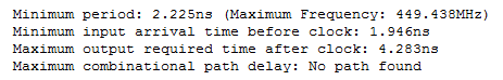
The hardware utilization summery after synthesis and MAP process may not match. The MAP process runs several optimization algorithms which remove or trims irrelevant, duplicate and unused logic elements. The maximum frequency achieved after synthesis process and after MAP process can be matched for smaller designs. But for complex designs generally the frequency achieved after MAP process is lower than the frequency achieved after synthesis process. The maximum frequency depends on the total delay time which can be expressed as
Total Delay = Data Path Delay (Logic Delay) + Clock Path Skew + Clock Uncertainty + Routing Path Delay
Device Programming
Now the design must be loaded on the FPGA. But the design must be converted to a format so that the FPGA can accept it. BITGEN program deals with the conversion. The routed NCD file is then given to the BITGEN program to generate a bit stream (a .BIT file) which can be used to configure the target FPGA device. This can be done using a cable. Selection of cable depends on the design.
Design Verification
Verification can be done at different stages of the process steps.
- Behavioral Simulation (RTL Simulation): This is the first of all simulation steps; those are encountered throughout the hierarchy of the design flow. This simulation is performed before synthesis process to verify RTL (behavioral) code and to confirm that the design is functioning as intended. Behavioral simulation can be performed on either VHDL or Verilog designs. In this process, signals and variables are observed, procedures and functions are traced and breakpoints are set. This is a very fast simulation and so allows the designer to change the HDL code if the required functionality is not met with in a short time period. Since the design is not yet synthesized to gate level, timing and resource usage properties are still unknown.
- Functional simulation (Post Translate Simulation): Functional simulation gives information about the logic operation of the circuit. Designer can verify the functionality of the design using this process after the Translate process. If the functionality is not as expected, then the designer has to made changes in the code and again follow the design flow steps.
- Functional simulation (Post PAR Simulation): Some time functional simulation works but design doesn’t produce the expected result when targeted to a FPGA device. This is due to the fact of rigorous optimization in the PAR process and failing to meet the constraints. Post PAR simulation can be run to check the functionality after PAR. It is expected that If the post PAR simulation is ok then the design can be successfully implemented.
- Static Timing Analysis: This can be done after MAP or PAR processes. Post MAP timing report lists signal path delays of the design derived from the design logic. Post Place and Route timing report incorporates timing delay information to provide a comprehensive timing summary of the design.
FPGA Editor
The FPGA Editor is a graphical application for displaying and configuring FPGAs. The FPGA Editor reads from and writes to NCD files, macro files (NMC), and PCF files.
The following is a list of a few functions that can be performed using FPGA Editor.
- Place and route critical components before running the automatic place and route tools.
- Finish PAR if the routing program does not completely route your design.
- Add probes to the design to examine the signal states of the targeted device. Probes are used to route the value of internal nets to an IOB (Input/Output Block) for analysis during the debugging of a device.
- Run the BitGen program and download the resulting bitstream file to the targeted device.
- View and change the nets connected to the capture units of an Integrated Logic Analyzer (ILA) core in your design.
- Create an entire design by hand (advanced users).
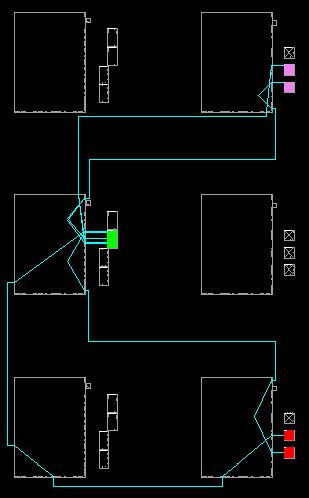
The following snapshot represents a fully routed implementation of a simple Half-Adder. The bigger rectangles are the programmable switch matrices. Total four IOBs are used and one CLB is occupied. The pink colored IOBs are for input and red colored IOBs are for output. The CLB is green colored.