Clock Domain Crossing (CDC) refers to the process and techniques used to manage data transfer between different clock domains within the digital system in either ASIC IC or FPGA. CDC is one where the data is transferred from one clock domain to another. A scenario of CDC is shown below in Figure 1. Here, data from clock domain A is transferred to clock domain B. Clock A and Clock B can be of different frequencies as well as of different phases. Thus two clock domains are asynchronous to each other. Data transfer from one clock-domain to another should be done very carefully so that no data should be lost.
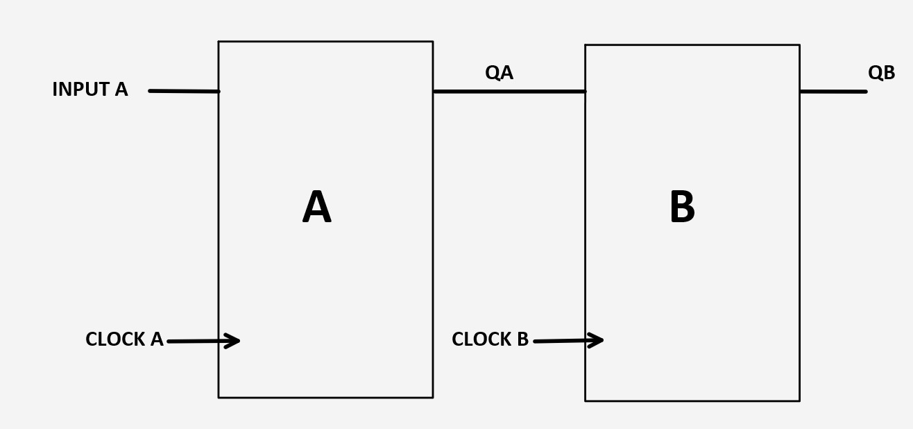
Modern ASICs often contain multiple clock domains, each operating at its frequency or phase. When data signals cross between these clock domains, it’s essential to ensure that the data transfer is done reliably and without errors. CDC mechanisms handle this task by synchronizing signals, managing timing constraints, and mitigating issues such as metastability, which can arise when signals transition between different clock domains.
Different subsystems within a System on Chip (SoC) usually run on different clocks and may have different reset signals. For example, a peripheral sub-system such as SPI may run on a slow 50 MHz clock while a high-performance CPU cluster will most likely run on a clock in the GHz range. For data to be transferred between these two different clock domains, clock (and reset) synchronization logic is required to be put in place at clock-crossing boundaries.
Problems in CDC
There are quite a few problems that arise while introducing multiple clock domains in ASIC. The main problem faced by engineers is called Metastability which is shown in Figure 2. Metastability occurs in applications that use multiple clock domains. There are a few important terms to know before delving deeper into this topic.
1) Setup Time – It is the window of time before the rising edge of the clock. Input must not change during this time.
2) Hold Time – It is the window of time that is after the rising edge of the clock. Output must not change during this time.
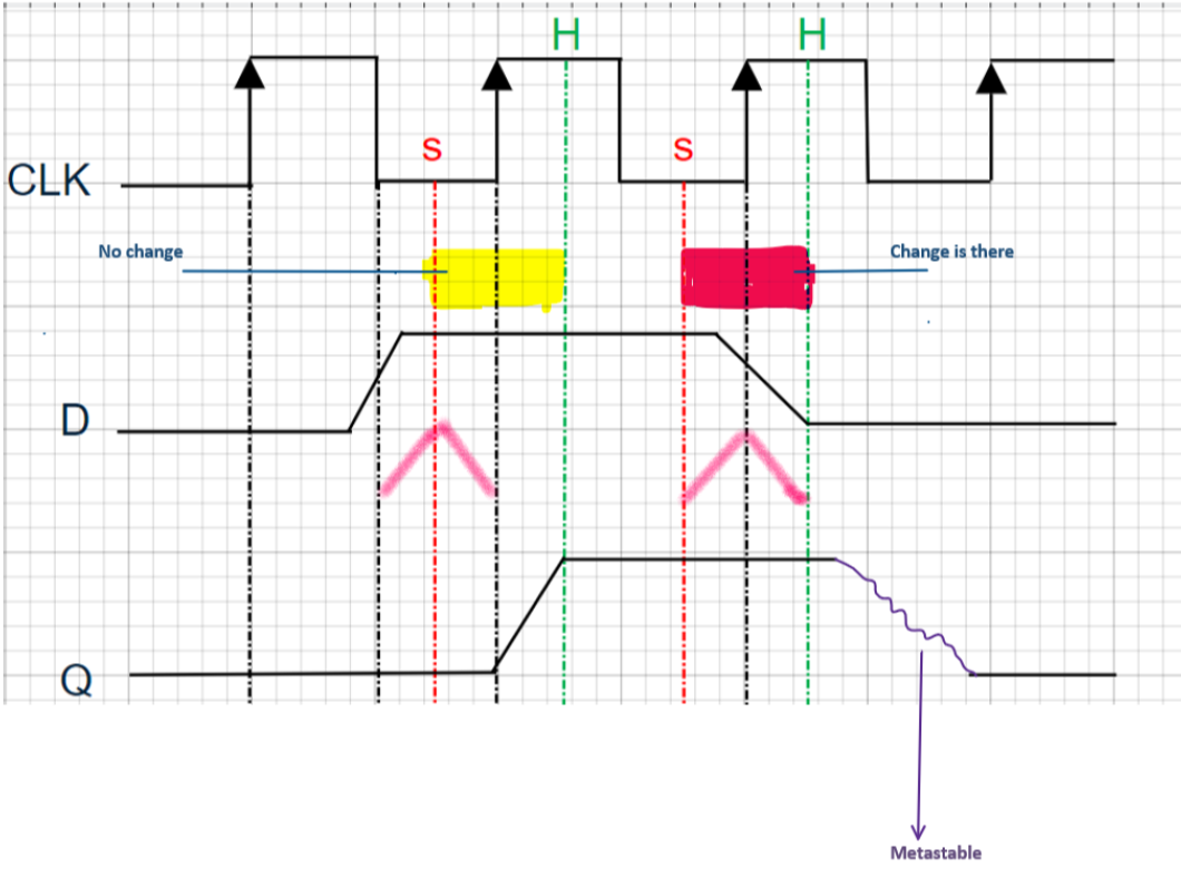
In the above diagram, CLK is the clock input, D is the data input, and Q is the output. Two regions will be considered here
The yellow-marked region
○ Input D gives an accurate output because the data is not changing for both the setup time and hold time
○ Accurate output is given according to the D input at the rising edge of the clock signal
The red-marked region
○ The input D has changed from 1 to 0 in the setup time
○ The output Q can be either 0 or 1 this unstable state is called the metastable state
It takes a long time to settle for a value of either 0 or 1. This leads to inaccurate outputs. Metastability holds huge consequences for State Machines as a single bit error can point to a completely different state and ruin the processes being carried out. Let’s discuss two cases of multiple cases, in one case data is transferring from a slow clock to a fast clock, and in another case, data is transferring from a fast to a slow clock.
Slow to Fast Clock Domain
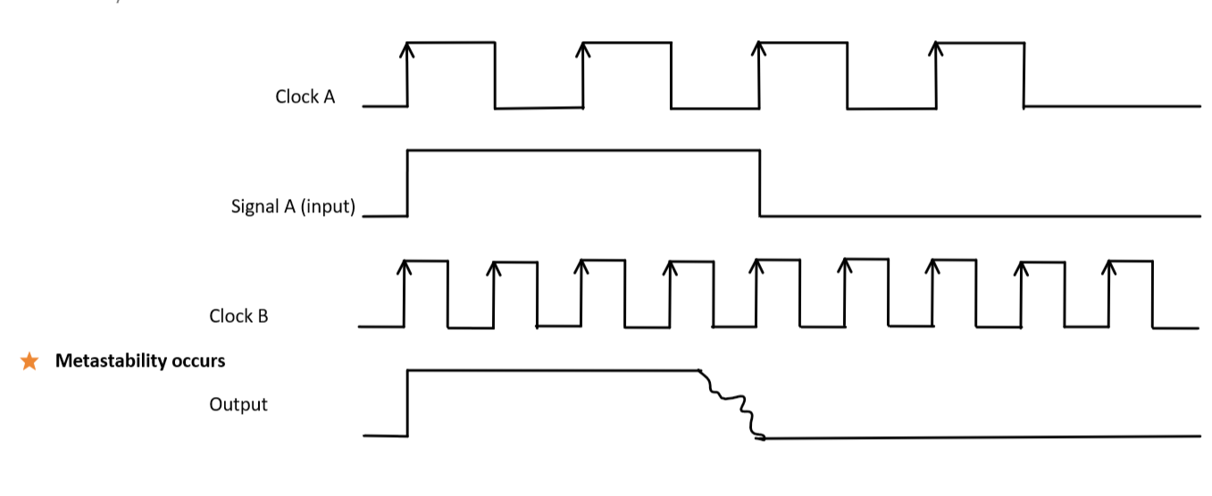
In this case, the source clock is slower than the destination clock. Let us consider an example where the source clock (clock A) and destination clock (clock B). Signal A is sampled multiple times by Clock B as it is faster assuming a metastable condition occurs due to unstable setup time and hold time as previously discussed The output is inaccurate and invalid to use. This scenario is shown in Figure 3 below.
Slow to Fast Clock Domain
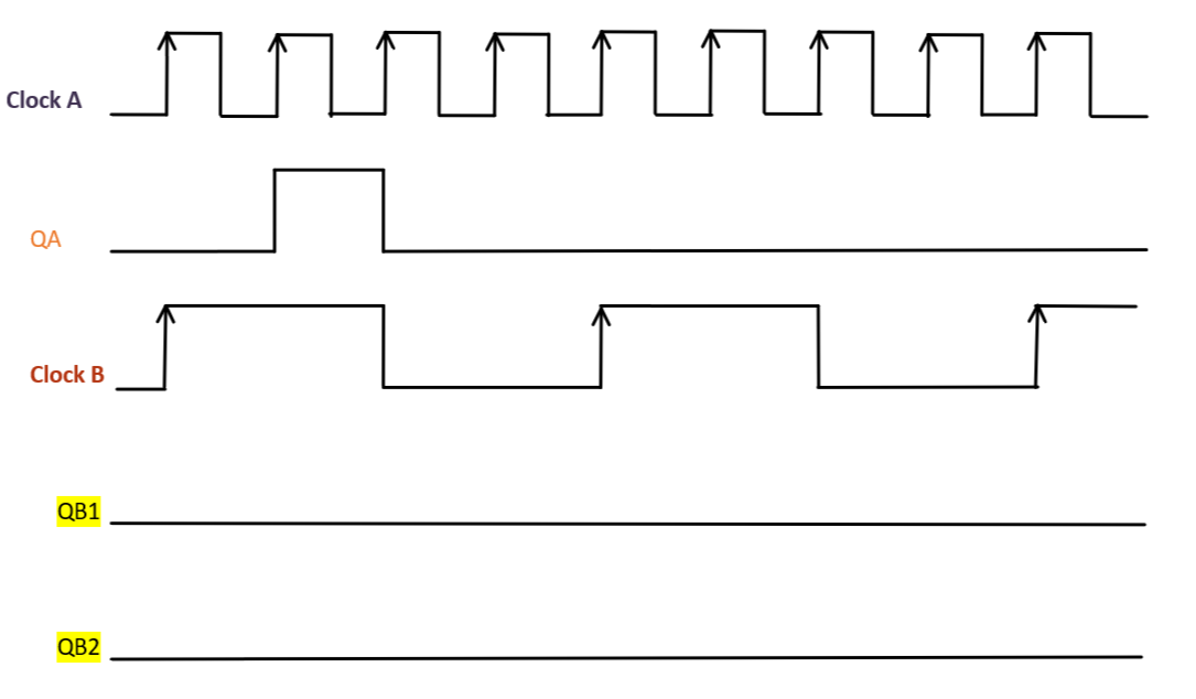
The second condition is when a system has a fast clock domain at the source and a slow clock domain at the destination. Let us consider this circuit shown in Figure 4.
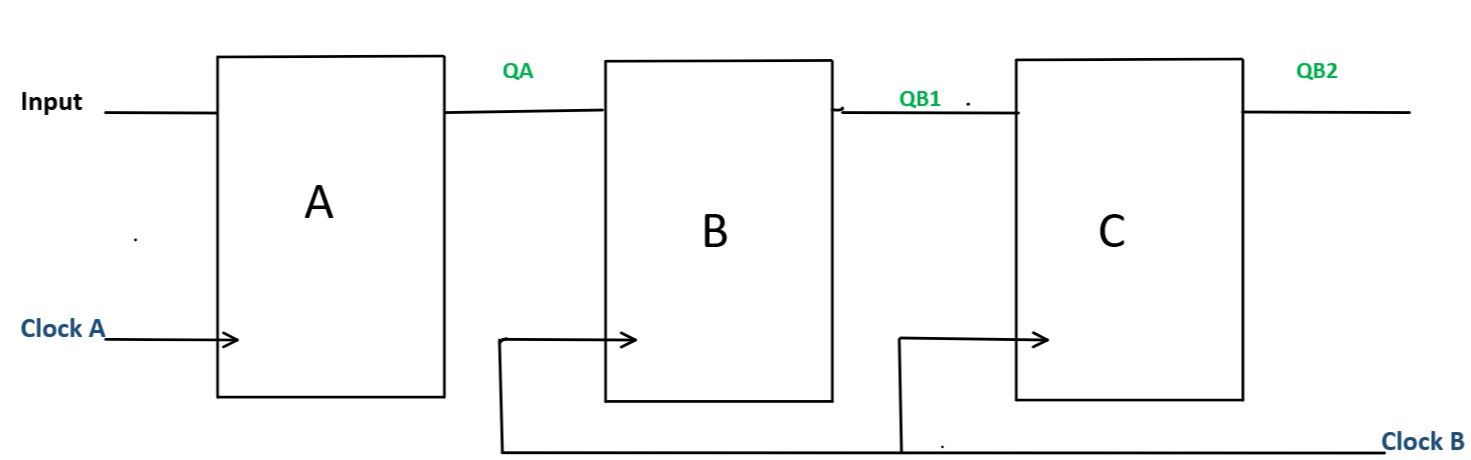
The slower clock misses the input signal QA due to its slower clock as shown in Figure 5. This happens because the rising edges of the slower clock i.e. Clock B are too far apart. Edge detection does not occur as it misses the start and end of the input signal QA. This results in the outputs at QB1 and QB2. The data is lost completely.
There are a few techniques that are proposed to avoid the problems in CDC and they are
- Two Flop Synchronizer
- Toggle Based Flop
- Handshake Mechanism
- Asynchronous FIFO
Author Details
Medha Satheesh is currently pursuing her B-Tech in electronics and communication (ECE) at Dayananda Sagar University, Bengaluru. She is a VLSI enthusiast and currently she is in 3rd year.