Artificial Neural Networks (ANN) are very popular to realize different critical functions related to any field of study. In this project, a simple exclusive-OR function is realized with the help of ANN. The purpose of the XOR function is to perform XOR operation between two inputs which can take value anything within the range -1 to 1. The output will be binary based on the values of the inputs. The ANN logic is explained here and finally, FPGA implementation of XOR function using ANN is demonstrated in this tutorial.
Three-level ANN architecture is used here. In the input level, there are two nodes named as  and
and  . In the hidden layer also we have two nodes named as
  and
and  . At the output, we have only one node named as
  . The architecture is shown below.
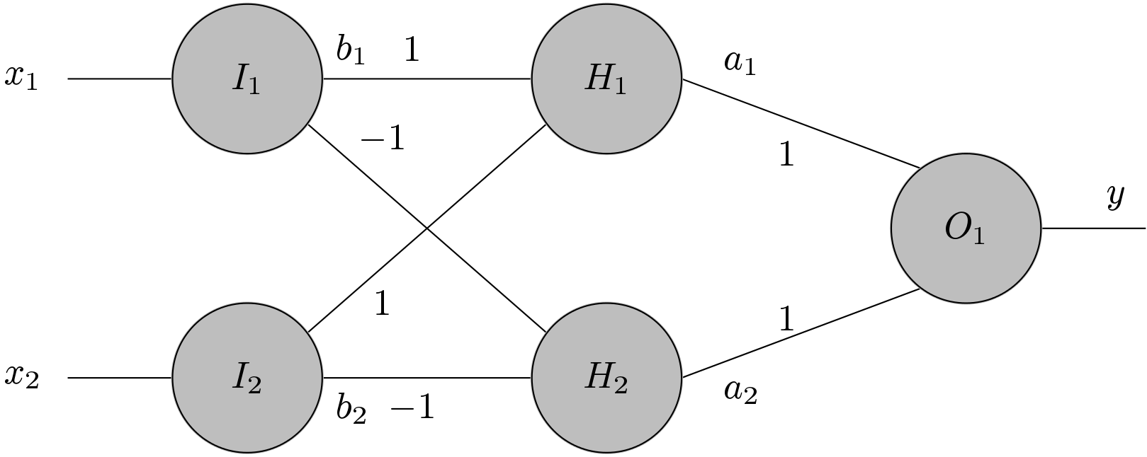
The input nodes follow the logic that is given below
(1) 
The logic of the Hidden layer nodes is given below.
(2) 
(3) 
Finally, the logic at the output node is given below.
(4) 
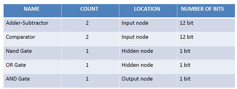
The ANN structure to realize the XOR function is implemented using the basic digital blocks and finally implemented on FPGA device. Fixed point arithmetic with the help of two’s complement representation is used here. The data width of 12 bits is used to represent the input data  where 10 bits are used for the fractional part. The digital hardware for the input nodes is shown below.
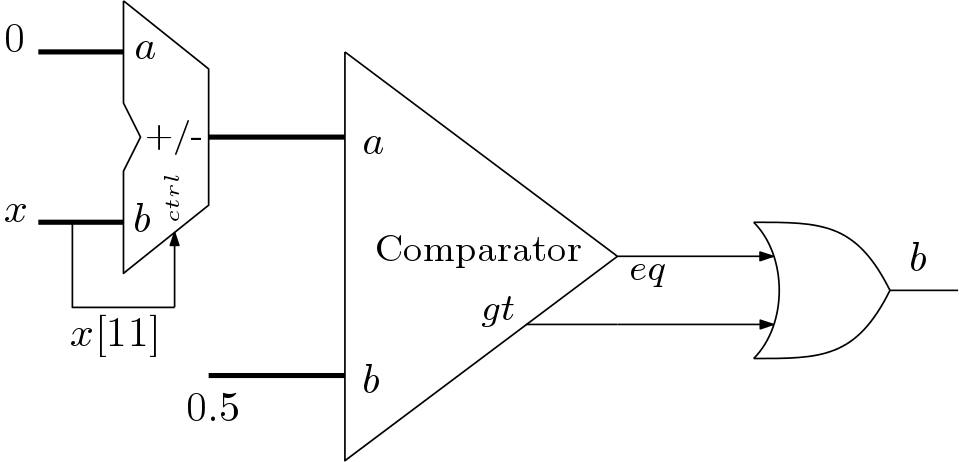
MSB of the input signal is used to perform either addition or subtraction before the comparator block. One input of the comparator is connected to 0.5 constantly. A 12-bit unsigned comparator is used here. The final and overall architecture is shown below
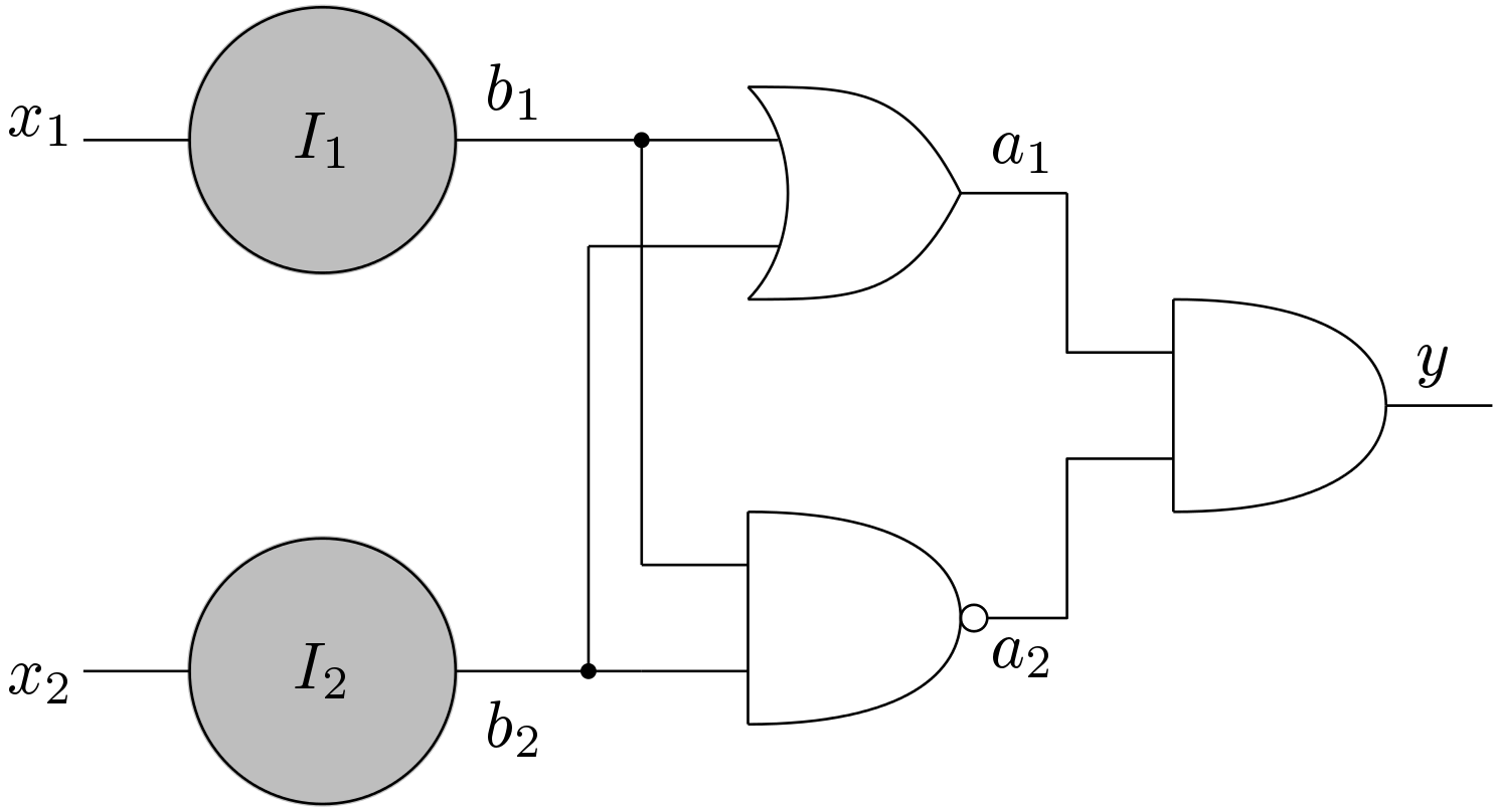
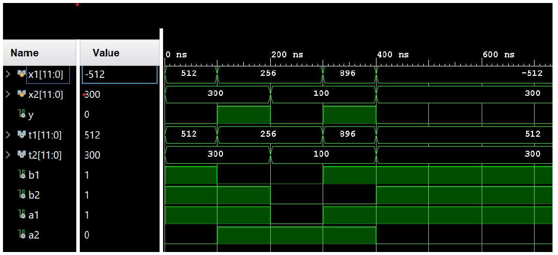
The architecture is very simple and self-explanatory. The overall architecture is implemented and verified using xc7a35tcpg236-2 FPGA. Simulation is done using the Xilinx-Vivado tool. The simulation result for the XOR implementation problem is shown below.
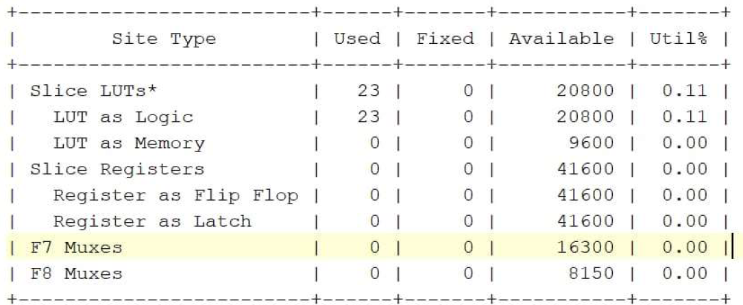
The hardware utilization report with respect to the targetted FPGA is shown below
This project was completed by the following students who are students of Dayandanda Sagar University.
- SHASHANK R
- SOURAV D
- SANKETH KUMAR
- PRITHIVRAJ Mulge