As we discussed in the previous blog one of the methods to solve metastability is the Double Flop Synchroniser method. This method consists of two cascaded D flip-flops that sample the input signal with the destination clock. This design can reduce the risk of metastability by adding a buffer stage between the source and the destination logic. The double flip-flop synchronizer can help mitigate the issues related to clock domain crossing (CDC) in data or control signals in any design.
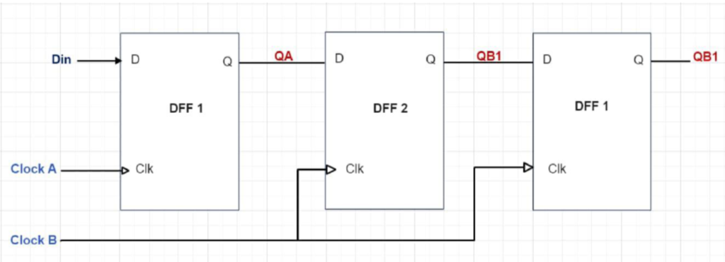
In the above figure, three flip-flops are used. Output of flip flop A is QA, Output of flip flop B is QB1, and Output of flip flop C is QB2. Input given to the flip-flop A will always be either 1 or 0. Output QA is given as input to B flip-flop. Flip-flop A is connected to clock A so output QA will reflect the rising edge of clock A. However we can see a change in the set-up time for signal QA when it reaches flip-flop B. This will result in a metastable state in the output QB. Now another flip flop C is connected whose input is QB. We must note that flip-flops B and C are connected to clock signal B. Adding flip-flop C gives buffer time. The purpose of adding this flip flop C is so that the output is delayed by one clock cycle. This ensures the point of metastability we had previously observed in QB1 is delayed thus producing accurate results.
Verilog Code for Double Flip-Flop Synchronizer
module d_ff (
    input clk,
    input d,
    output reg q
);

always @(posedge clk)
begin
    q <= d;
end

endmodule

module d_ff_chain (
    input clkA,
    input clkB,
    input d,
    output  qa, // Output of the first D flip-flop
    output  qb1, // Output of the second D flip-flop
    output qb2 // Output of the third D flip-flop
);
wire intermediate_q1, intermediate_q2;

// Instantiate the first D flip-flop controlled by clkA
d_ff dff1 (
    .clk(clkA),
    .d(d),
    .q(qa) // Rename the output to qa
);

// Instantiate the second D flip-flop controlled by clkB
d_ff dff2 (
    .clk(clkB),
    .d(qa), // Connect to the output of the first D flip-flop
    .q(qb1) // Rename the output to qb1
);

// Instantiate the third D flip-flop controlled by clkB
d_ff dff3 (
    .clk(clkB),
    .d(qb1), // Connect to the output of the second D flip-flop
    .q(qb2) // Rename the output to qb2
);

endmodule
module tb;
// Inputs
reg clkA;
reg clkB;
reg d;
// Outputs
wire qa;
wire qb1;
wire qb2;
// Instantiate the Unit Under Test (UUT)
d_ff_chain uut (
.clkA(clkA),
.clkB(clkB),
.d(d),
.qa(qa),
.qb1(qb1),
.qb2(qb2)
);
initial
begin
// Initialize Inputs
clkA = 1'b0;
clkB = 1'b1;
d = 1'b1;
end
always #10 clkA =~clkA;
always #10 clkB = ~clkB;
initial begin
#20 d = 1'b0;
#20 d = 1'b1;
#20 d = 1'b0;
#20 d = 1'b1;
#20 d = 1'b0;
#20 d = 1'b1;
#20 d = 1'b0;
#20 d = 1'b1;
#20 d = 1'b0;
#20 d = 1'b1;
#20 d = 1'b0;
#20 d = 1'b1;
end
endmoduleSimulation Results
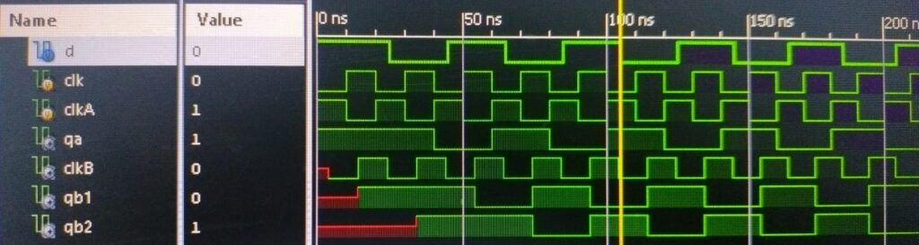
Three cases are studied for the double flip-flop synchronizer to solve CDC issues. These cases are shown below
1. Source and destination clocks are of same frequency but of different phases.
2. The source clock is slower than destination clock
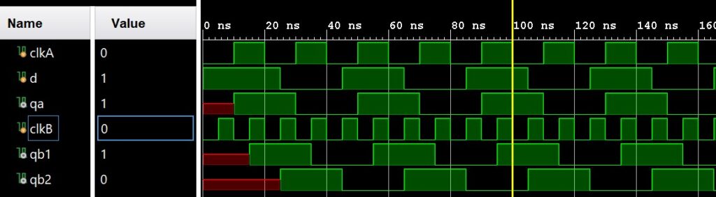
In this scenario, destination clock speed is two times faster than the source clock. Data signal is aligned with the positive edge of the destination clock but width of the data signal is twice the width of clock signal.
3. The source clock is faster than destination clock
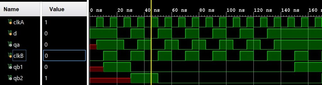
In this scenario, double flip-flop technique fails to solve the CDC issue. Data cannot be transferred faster domain to slower domain.