An FPGA is a device that contains a matrix of reconfigurable gate array logic circuitry. When a FPGA is configured, the internal circuitry is connected in a way that creates a hardware implementation of the software application. Unlike processors, FPGAs use dedicated hardware for processing logic and do not have an operating system. FPGAs are truly parallel in nature and hence different processing operations do not have to compete for the same resources
FPGAs are based on an array of logic modules and a supply of uncommitted wires to route signals. In gate arrays these wires are connected by a mask design during manufacture. In FPGAs, however, these wires are connected by the user and therefore must use an electronic device to connect them. Three types of devices have been commonly used to do this, pass transistors controlled by an SRAM cell, a flash or EEPROM cell to pass the signal, or a direct connect using antifuses. Each of these interconnect devices have their own advantages and disadvantages. This has a major affect on the design, architecture, and performance of the FPGA. Classification of FPGAs on user programmable switch technology is described below
Anti-fuse Based – All the contacts are open initially. Programming converts selected locations as conducting. This process is One time programmable (OTP). Further, this technology is non-volatile in nature and does not make use of standard CMOS process.
SRAM Based – Static memory cells are the basic cells used for SRAM-based FPGAs. Most commercial vendors use static memory (SRAM) based programming technology in their devices. These devices use static memory cells which are divided throughout the FPGA to provide configurability. In an SRAM-based FPGA, SRAM cells are mainly used for following purposes:
- To program the routing interconnect of FPGAs which are generally steered by small multiplexors.
- To program Configurable Logic Blocks (CLBs) those are used to implement logic functions.
SRAM-based programming technology has become the dominant approach for FPGAs because of its re-programmability and the use of standard CMOS process technology and therefore leading to increased integration, higher speed and lower cost.
E2ROM or Flash based – This programming technology is nonvolatile in nature. Flash-based programming technology is also more area efficient than SRAM-based programming technology. Flash-based programming technology has its own disadvantages also. Unlike SRAM based programming technology, flash based devices cannot be reconfigured/reprogrammed for infinite number of times. Also, flash-based technology uses non-standard CMOS process.
Tradeoffs: Anti-fuse technology consumes less area and less power. E2RAM takes more time for programming. SRAM is technology leaders in Programmable Logic devices.
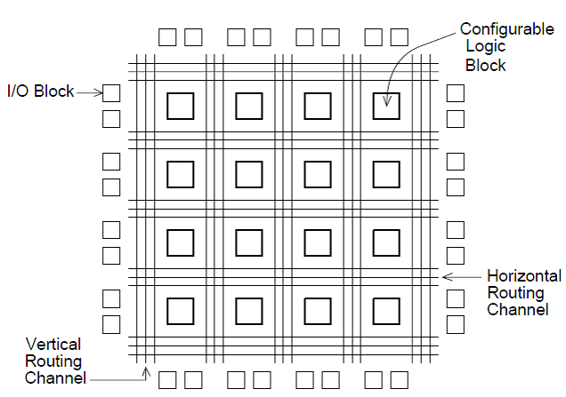
The FPGA consists of three major components as shown in Fig. 1.
- Configurable Logic Blocks (CLB), which implement logic functions
- I/O blocks (IOB), which are used to make off-chip connections
- Programmable Routing (interconnects), which connects I/O blocks and CLBs
Configurable Logic Blocks (CLB)
Configurable Logic Block (CLB) is a fundamental building block of FPGA technology. Any logic circuit can be realized in terms of these CLBs. A CLB can be based on basic logic gates, mux based or LUT based depending upon the technology. The granularity of the reconfigurable logic is defined as the size of the smallest functional unit (CLB). Depending on the granularity, reconfigurable devices can be of following types.
- Fine Grained – A universal gate like NAND or AND-OR-NOT, are basic block.
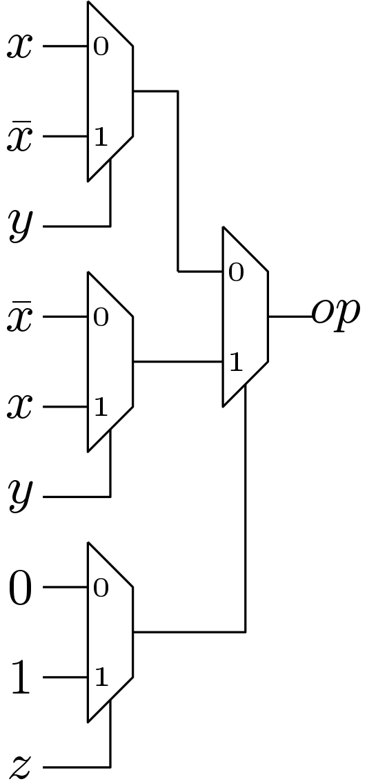
- Middle Grained – CLBs are either Multiplexer based (Fig. 3) or ROM/RAM based (Fig. 2).
- Coarse Grained – FFT or a processor work as a basic unit.
Tradeoffs: Fine grain FPGA involves more interconnection overhead whereas coarse grain reconfigurable devices are application specific.
Two type of CLBs are shown below which implements the function 
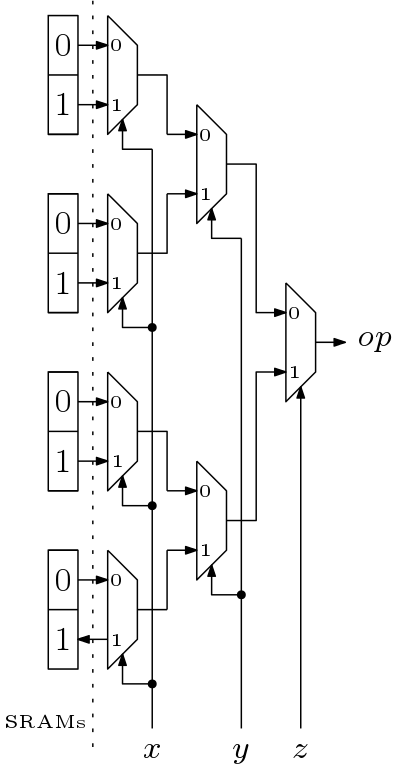
Fig. 2: An LUT Based CLB Programmed by SRAM
CLBs consist of Look-up Tables (LUT) which implements the entries of a logic function’s truth table. Some FPGAs can use LUTs to implement small Random Access Memory (RAM). CLBs has Carry and Control Logic which Implements fast arithmetic operations (adders/ subtractors). CLBs can be also configured for additional operations (Built-in-Self Test iterative-OR chain) and have configurable Flip Flops (FFs)/ Latches (Programmable clock edges, set/reset, and clock enable). These memory elements usually can be configured as shift-registers.
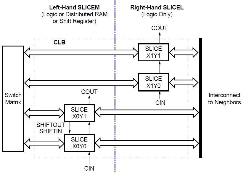
Each CLB of Spartan 3E (xc3s500e) FPGA comprises four interconnected slices, as shown in Fig. 4. These slices are grouped in pairs and each pair is organized as a column with an independent carry chain. The left pair supports both logic and memory functions and its slices are called SLICEM. The right pair supports logic only and its slices are called SLICEL. Therefore half the LUTs support both logic and memory (including both RAM16 and SRL16 shift registers) while half support logic only, and the two types alternate throughout the array columns. The SLICEL reduces the size of the CLB and lowers the cost of the device, and can also provide a performance advantage over the SLICEM.
Slice Overview: A slice includes two 4 input LUT function generators (G and F) and two programmable storage elements along with additional logic circuitry, as shown in Fig. 5. Both SLICEM and SLICEL have the following elements in common to provide logic, arithmetic and memory functions:
- Two 4-input LUT function generators, F and G
- Two storage elements
- Two wide-function multiplexers, F5MUX and FiMUX
- Carry and arithmetic logic
The SLICEM pair supports two additional functions:
- Two 16×1 distributed RAM blocks, RAM16
- Two 16-bit shift registers, SRL16
Realization of a half-adder with inputs a and b is shown in Fig. 5. The sum output of the half-adder is computed by G-LUT and carry out (co) output is computed by F-LUT. The red line are connected to realize the half-adder.
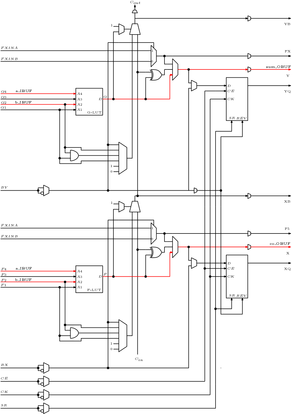
Fig. 5: Spartan 3E SLICE Architecture
Logic Cells: The combination of a LUT and a storage element is known as a “Logic Cell”. The additional features in a slice, such as the wide multiplexers, carry logic and arithmetic gates enhances the capacity of a slice. Benchmarks have shown that the overall slice is equivalent to 2.25 simple logic cells.
Input/Output Block (IOB)
The Input/Output Block (IOB) provides a programmable, unidirectional or bidirectional interface between a package pin and the FPGA’s internal logic, supporting a wide variety of standard interfaces. The robust feature set includes programmable control of output strength and slew rate, registered or computational inputs and outputs with dedicated double data rate (DDR) registers, programmable input delays, on-chip termination, and hot-swap capability. There are three main signal paths within the IOB: output path, input path, and 3-state path.
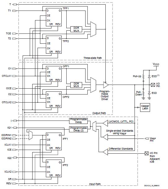
Each path has its own pair of storage elements that can act as either registers or latches.
- The input path carries data from the pad, which is bonded to a package pin, through an optional programmable delay element directly to the I line. After the delay element, there are alternate routes through a pair of storage elements to the IQ1 and IQ2 lines. The IOB outputs I, IQ1, and IQ2 lead to the FPGA’s internal logic. The delay element can be set to ensure a hold time of zero.
- The output path, starting with the O1 and O2 lines, carries data from the FPGA’s internal logic through a multiplexer and then a three-state driver to the IOB pad. In addition to this direct path, the multiplexer provides the option to insert a pair of storage elements.
- The 3-state path determines when the output driver is high impedance. The T1 and T2 lines carry data from the FPGA’s internal logic through a multiplexer to the output driver. In addition to this direct path, the multiplexer provides the option to insert a pair of storage elements. All signal paths entering the IOB, including those associated with the storage elements, have an inverter option. Any inverter placed on these paths is automatically absorbed into the IOB.
Programmable Interconnect
Interconnect is the programmable network of signal pathways between the inputs and outputs of functional elements within the FPGA, such as IOBs, CLBs, DCMs, and block RAM. Interconnect, also called routing, is segmented for optimal connectivity. There are four kinds of interconnect: long lines, hex lines, double lines, and direct lines.
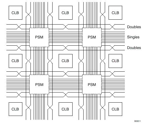
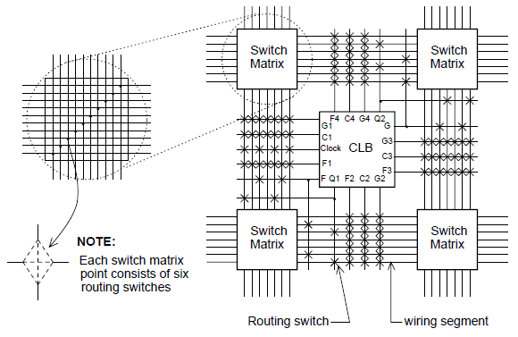
Programmable Switch Matrix (PSM): The switch matrix (Fig. 8) connects to the different kinds of interconnects across the device. An interconnect tile is defined as a single switch matrix connected to a functional element, such as a CLB, IOB, or DCM. If a functional element spans across multiple switch matrices such as the block RAM or multipliers, then an interconnect tile is defined by the number of switch matrices connected to that functional element. The four types of interconnect lines are described below.
Long Lines: Each set of 24 long line signals spans the die both horizontally and vertically and connects to one out of every six interconnect tiles. At any tile, four of the long lines drive or receive signals from a switch matrix. Because of their low capacitance, these lines are well-suited for carrying high frequency signals with minimal loading effects (e.g. skew). If all global clock lines are already committed and additional clock signals remain to be assigned, long lines serve as a good alternative.
Hex Lines: Each set of eight hex lines are connected to one out of every three tiles, both horizontally and vertically. Thirty-two hex lines are available between any given interconnect tile. Hex lines are only driven from one end of the route.
Double Lines: Each set of eight double lines are connected to every other tile, both horizontally and vertically in all four directions. Thirty-two double lines available between any given interconnect tile. Double lines are more do connections and of more flexibility, compared to long line and hex lines.
Direct Connections: Direct connect lines route signals to neighboring tiles: vertically, horizontally, and diagonally. These lines most often drive a signal from a “source” tile to a double, hex, or long line and conversely from the longer interconnect back to a direct line accessing a “destination” tile.