In the previous tutorial on Placement And Routing For ASIC, we have seen that one I/O file is also important. This tutorial is on I/O file setup for PnR using INNOVUS. An I/O file is for custom arrangement of I/O pins and I/O pads. This file is optional if the final sign-off analysis is not to be performed using INNOVUS. In this case tool will assign the I/O pins in a convenient order.
I/O Planning
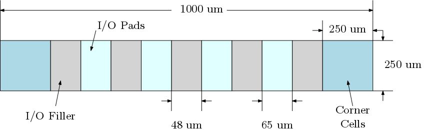
Planning of input and output pins or pads is very important. Earlier we have seen that Corner cells are placed at the four corners of an IC. The dimension of corner cells for our technology is ( ). The I/O pads have dimension of (
 ). This means the I/O pads have width of 65 um. In the case of the simple 4-bit counter there are 4 I/Os at each side. Say, the total area for the IC is
  . Then the gap between the I/O pads is X. The value of X can be found out as

Thus 
This is shown in Figure 1
Pad Connectivity
The details of I/O pins arrangement and I/O pads are given in I/O file but the connectivity of these PADS with the actual inputs and outputs is not done yet. This connectivity is done using the Gate Level Netlist file. The detail about the different I/O pads can be found in the technological libraries. Verilog models of these I/O pads are also available in the Library. These Verilog models are instantiated in the Netlist file to be connected with actual I/Os. An example of this type of connectivity is shown below.
(globals
	version = 3
	io_order = clockwise
	space = 48
	total_edge = 5
)
(iopad
	(topleft
		(inst name="CornerCell1" cell=pfrelr offset=0 orientation = R180 place_status = fixed))
	(left 	(inst name="Iclk" cell=pc3d01 place_status = fixed)
		(inst name="Ien" cell=pc3d01 place_status = fixed)
		(inst name="Irst" cell=pc3d01 place_status = fixed)
		(inst name="POWER_VDDO1" cell=pvdi place_status = fixed)

	)
	(topright
		(inst name="CornerCell2" cell=pfrelr offset=0 orientation = R90 place_status = fixed))
	(top 	(inst name="out1" cell=pc3d01 place_status = fixed)
		(inst name="out2" cell=pc3d01 place_status = fixed)
		(inst name="POWER_VDD02" cell=pc3d01 place_status = fixed)
		(inst name="POWER_VSS02" cell=pv0i place_status = fixed)
	)
	(bottomright
		(inst name="CornerCell3" cell=pfrelr offset=0 orientation = R0 place_status = fixed))
	(right 	(inst name="out3" cell=pc3d01 place_status = fixed)
		(inst name="out4" cell=pc3d01 place_status = fixed)
		(inst name="POWER_VDD03" cell=pc3d01 place_status = fixed)
		(inst name="POWER_VSS03" cell=pv0i place_status = fixed)
	)
	(bottomleft
		(inst name="CornerCell4" cell=pfrelr offset=0 orientation = R270 place_status = fixed))
	(bottom (inst name="IscanI" cell=pc3d01 place_status = fixed)
		(inst name="IscanE" cell=pc3d01 place_status = fixed)
		(inst name="IscanO" cell=pvda place_status = fixed)
		(inst name="POWER_VSSO1" cell=pv0i place_status = fixed)
	)
)
Gate Level Netlist File of Simple counter is modified for I/O pad connectivity.
// Generated by Cadence Genus(TM) Synthesis Solution GENUS15.21 - 15.20-s010_1
// Generated on: Mar 17 2020 19:57:19

// Verification Directory fv/OMP_K16_N128_ff4_16bit

module counter(clk,reset,en,scan_in,scan_en,scan_out,out);
input clk,reset,en,scan_in,scan_en;
output [3:0] out;
output scan_out;

wire clk1,reset1,en1,scan_in1,scan_en1,scan_out1;
wire [3:0] out1;

counter cnt(clk1, reset1, en1, scan_in1, scan_en1, scan_out1,
     out1);

pc3d01 Irst(.PAD(reset),.CIN(reset1));
pc3c01 Iclk(.CCLK(clk),.CP(clk1));
pc3d01 Ien(.PAD(wr_ym),.CIN(wr_ym1));

pc3d01 IscanI(.PAD(scan_in),.CIN(scan_in1));
pc3d01 IscanE(.PAD(scan_en),.CIN(scan_en1));
pc3d01 IscanO(.PAD(scan_out1),.CIN(scan_out));

pc3d01 out1(.PAD(out1[0]),.CIN(out[0]));
pc3d01 out2(.PAD(out1[1]),.CIN(out[1]));
pc3d01 out3(.PAD(out1[2]),.CIN(out[2]));
pc3d01 out4(.PAD(out1[3]),.CIN(out[3]));
endmodule