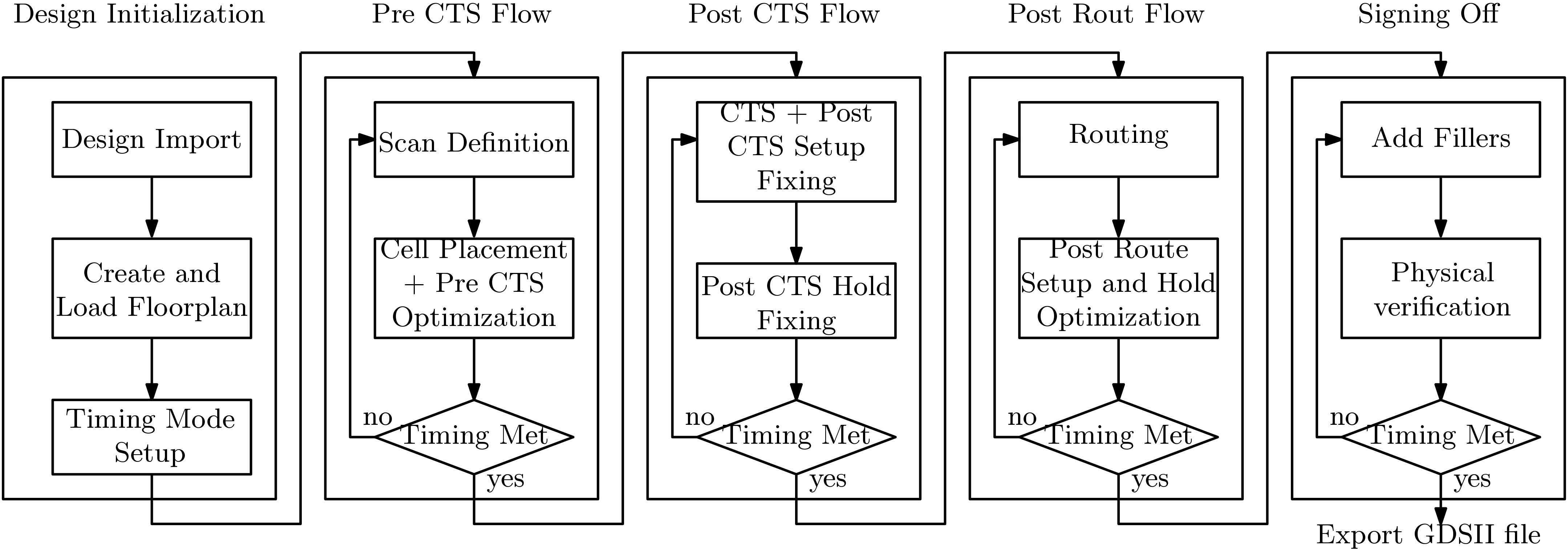
The previous tutorials [Tutorial 1, Tutorial 2] are on the simulation and synthesis of Verilog files. In addition to these we have also performed linting, code coverage, logic equivalence check, DFT, ATPG, power analysis and Timing analysis using CADENCE and SYNOPSYS tools. Till now we have not discussed anything about the step Placement and Routing for ASIC. In the implementation step, the design netlist file is mapped using the standard cells specified by a certain technology. This tutorial is on basic flow for Placement and Routing for ASIC. The basic Placement and Routing for ASIC flow is shown below
In this tutorial, we will use CADENCE INNOVUS tool for placement and Routing. We will provide very basic tutorials on how to perform placement and routing using INNOVUS and these are
- Importing Files for PnR using INNOVUS
- MMMC file setup for PnR using INNOVUS
- IO file setup for PnR using INNOVUS
- Placement and Routing using INNOVUS
- PnR using INNOVUS with scripts
Now let’s discuss the basic overview of ASIC implementation flow.
Design Initialization
The first step of the design initialization is design import. The Verilog Netlist flie, created after the synthesis step is the main design file to the PnR tool. Only the Netlist file is not enough for the PnR tool. There are other associated files which should be imported along with the Netlist file. These files are
- LEF Files:- Library Exchange Format (LEF) is a specification for representing the physical layout of an integrated circuit in an ASCII format. It includes design rules and abstract information about the cells. There are three kinds of LEF files which are Technology LEF File, Standard Cell LEF file, IO LEF file.
- IO Assignment File – This file helps the tool for custom assignment of IO pins and PADs.
- Multi-Mode Multi Corner (MMMC) View Definition File:- The MMMC view definition file contains pointers to two type of files which are Liberty Timing Models Files (LIB), Design Constraints (SDC). LIB files contain timing information about the standard cells and IO pads and SDC file contains the different timing constraints.
- Power Management Files: Common Power Format (CPF) file is an additional file for low power design.
- Graphic Design System (GDSII Files): These files are required for layout extraction. There are two type of GDSII files, technology GDS and I/O pad GDS. At the time of layout generation, these GDS files are merged to produce actual GDS fille of the IC.
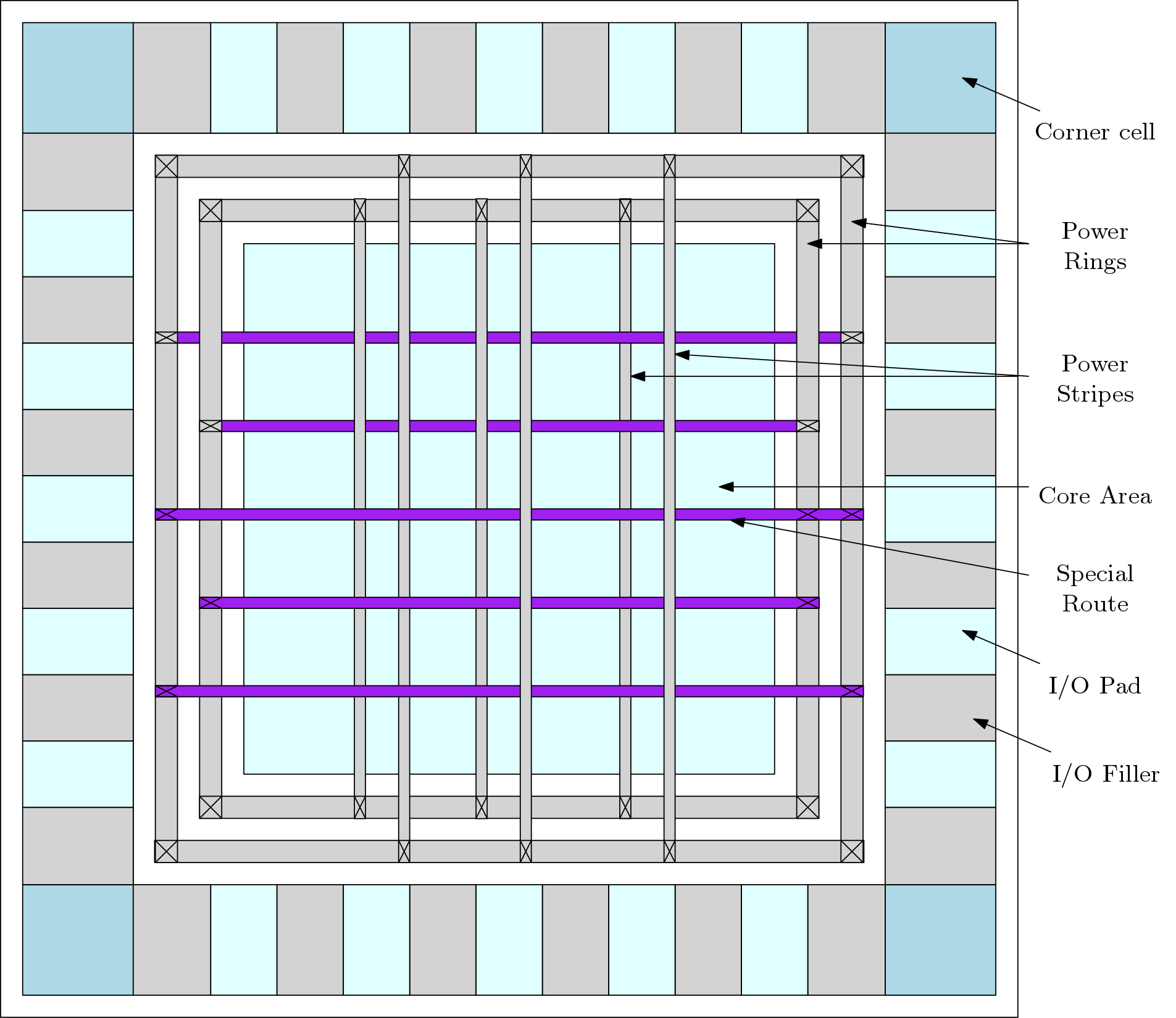
Create and Load Floor plan: Once the design files are loaded, the PnR tool can automatically calculates the area and load a floor plan based on the core utilization factor. Core utilization factor is defined as the ratio of the area of the design (area of the standard cells + area of the macro cells) to the core area. The designers can also specify the dimension for the floor plan.
A simplified floor-plan is shown in Figure 2 where floor plan is divided in two area viz., Core area and the IO ring around the core area. The Rings are carrying Vdd and Gnd around the core area. The stripes take connection of Vdd and Gnd inside the Core area. The special routes provide Vdd and Gnd connection to each cell in the Core area. In the Figure 2, the IO ring is also shown. The blocks at the four corners are called as Corner cells. Different orientations of the corner cells are available in the IO library.
Pre-CTS Flow
First step that is to be performed in this flow is to check for scan path functionality. Generally the scan cells are defined in the timing libraries but in this stage scan cells can also be defined. The scan cells and the scan chains are inserted in netlist in the synthesis stage. If one do not want to retain the scan chain order in the design, can change the order of the scan flip-flops which are connected along the scan chain for any scan groups. This process changes the connection constraints of scan cells but not the placement constraints. The reordering of scan chains can be performed in two ways
- Native Scan Reordering Approach – This method is applicable when the designer does not have scandef file. In this approach, the designers have to specify regarding the scan cells, scan chains and scan paths.
- Scandef Method – This approach reorders the scan chains with the help of scandef file. This method is preferred by Cadence tool as it is easier to execute.
Once the scan cells are configured, the design can be placed. The tool offers various optimization steps for the design. The design can be placed with or without optimization. Once the optimization step executes, the design is checked for timing. Timing checks are checks to see whether the design meets the setup and hold criteria. If the designs meet the timing then the post CTS flow can be started else designer may choose to improve the modifications in Pre-CTS flow or in the design initialization step.
Post-CTS Flow
Clock Tree Synthesis (CTS) is a very important operation that must be successfully run. CTS is a process of building physical structure between the clock source and all the sink flip-flops. It is always performed after placing the standard cells that is after fixing the location of the standard cells. CTS ensures that the clock signal is distributed evenly to all the sequential elements.
The goal of the CTS is to meet the
- Design Rule Constraints (DRC) – Maximum transition delay, maximum load capacitance and maximum fanout
- Clock tree targets – Maximum skew, min/max insertion delay.
The CTS step ensures the following parameters
- Clock skew should be at minimum.
- There should not be any pulse width and duty cycle violation.
- Clock latency should be minimum
- Clock tree power should be at minimum. Minimum power is achived by minimizing the transition and latency.
- Minimizing the signal crosstalk.
CTS archive these targets by choosing suitable clock tree algorithms which are H-Tree, C-Tree, Method of Mean and Median, Geometric Matching Algorithms, Pi Configuration. An example of classic H-clock tree structure is shown in Figure. The clock tree optimization techniques are
- Buffer and gate sizing – Buffers and the gates are sized up or down to improve skew and insertion delay.
- Buffer and Gate Relocation – Location of the buffers and gates are relocated to improve timing performance.
- Level Adjustment– Level of the clock pins can be adjusted t upper or lower level.
- Reconfiguration – Sequential elements can be clustered and then the buffer placement can be done.
- Delay Insertion – Provision of delay insertion is there for shorter paths.
- Dummy load insertion – The load balancing is done by inserting dummy loads.
Once CTS step is successfully performed, the timing checks are performed. Meeting the setup timing constraints depends on the delay of the critical path. CTS takes care that the max path does not get much delay. CTS tries to fix the hold problem by inserting buffers in the min paths. Fixing the hold slack also can violate the setup condition. If the timing is met, the routing can be started or the previous steps can be run again.
Post-Route Flow
Based on the logical connectivity, physical connections are made between the cells in the routing flow. The routing is done in a way that the paths should meet the constraints. There are actually three types of routing which are
- Power Routing – Routing of power nets are partially done in floor planning stage but connection of Vdd and Gnd pins of a cell is performed in the routing flow.
- Clock routing – Clock tree is formed and reorganized in the CTS flow. In the routing stage, leaf nodes in tree are connected to clock signal.
- Signal routing – All the signal nets are routed in this stage. The critical nets can be routed in a special way if mentioned.
The overall routing job is executed in three steps which are
- Global Routing – In this stage, the whole design is first partitioned in small routing region into tiles/rectangles. Also, region to region paths are decided in a way to optimize the wire lengths and timing. This stage is actually the planning stage and no actual routing is done.
- Track Assignment – In this stage, the routing tracks assigned by the global stage are replaced by the metal layers. Tracks are assigned in horizontal and vertical direction. If overlapping is occurred then rerouting is done.
- Detailed Routing – Even if the metal layers are laid, the path may exists which can violate the setup and hold criteria In this stage, the critical paths are searched and fixed in many iterations until fixed.
Sign-Off Flow
After routing we can proceed to the signing Off stage if the constraints are met or constraints are not met by small margin. Signing Off stage is the last stage of physical implementation of an IC. First step to be performed in this flow is to add filler cells in core area and in the IO ring. Various size of filler cells are available in library. In the next stage, the following checks are performed
- Logical Checks – Two types of logical checks are performed which are Logic Equivalence Check (Verilog vs Netlist) and Timing Checks (Setup and Hold check)
- Physical Checks – The physical checks which are mandatory to perform are Layout Versus Schematic (LVS) Check, Design Rule Checks (DRC), Electrical Rule Checks (ERC), Antenna Check,
- Power Checks – The power checks are Dynamic IR drop check, Electromigration (ER) check.
Once all the physical checks are successfully verified, the design is now ready for fabrication. The layout of the IC can now be generated in the GDSII format. This format can be sent to the foundry for fabrication.