Contents for memory design are
- Controlled Register
- Read Only Memory (ROM)
- Random Access Memory (RAM)
- Dual Port Memory
- Simple Dual Port Memory
In digital system design, the usage of memory elements is unavoidable. In some of the systems, data can be pre-stored in a constant memory. Memory elements can be used as temporary storage of intermediate data. Memory elements can also be used to realize any logic function.
In this tutorial, the realization of different types of memory blocks using Verilog is discussed. Though there are only 2 types of memory block exists, we divided memory blocks into four types according to their usage. Those are
- Controlled Register
- Single port Read Only Memory (ROM)
- Single port Random Access Memory (RAM)
- Dual port memory elements
Go to the Top
Controlled Register
Controlled registers can be considered as basic elements of larger memory blocks. It has a Control Enable (CE) input along with reset, preset inputs. When CE is high, data is loaded or data is written into this control register and output remains unchanged until any change in CE input. The usage of control registers is useful when we want to store a data vector or a scalar data. This saves the limited numbers of inbuilt memory blocks. The block diagram of a control register is shown below.
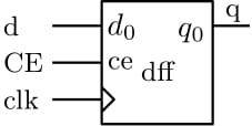
Fig. 1: Controlled Register
Single port Read Only Memory (ROM)
Read Only Memory (ROM) is a constant memory. The usage of this type of memory is obvious. ROM can be used to hold initial data for a system to start. A simple Verilog code for a single port ROM is shown below. Here initial data are loaded in the array locations using the case statement. The en input is sometimes optional but it is preferred to use en input to disable the memory block when not in use.
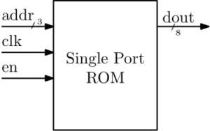
Fig. 2: Single Port ROM
module rom(clk,addres,data_out,en);

input clk,en;

input [2:0] addres;

output reg [7:0] data_out;

reg [7:0] mem [0:7];

initial begin data_out = 8'b00000000; end

always @ (addres)

case (addres)

3'b000 : mem[addres] = 8'b00000001;

3'b001 : mem[addres] = 8'b00000010;

3'b010 : mem[addres] = 8'b00000011;

3'b011 : mem[addres] = 8'b00000100;

3'b100 : mem[addres] = 8'b00000101;

3'b101 : mem[addres] = 8'b00000110;

3'b110 : mem[addres] = 8'b00000111;

3'b111 : mem[addres] = 8'b00001000;

default : mem[addres] = 8'b0000000;

endcase

always@(posedge clk)

begin

if(en)begin

data_out <= mem[addres];

end else

data_out <= data_out;

end

endmodule

Go to the Top
Single port Random Access Memory (RAM)
Random Access Memory (RAM) blocks are used to store data temporarily in a digital system. In a single port RAM, writing and reading can be done through one port only. It has one en input and we input. When en and we are both high, data are written into RAM and if en is high but we is low, reading through RAM can be done. The block diagram and Verilog code of a RAM block is shown below.
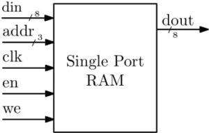
Fig. 3: Single Port RAM
module ram(clk,addres,data_in,en,we,data_out);

input clk,en,we;

input[2:0] addres;

input[7:0] data_in;

output reg [7:0] data_out;

reg [7:0] mem [0:7];

initial begin data_out = 8'b00000000; end

always@(posedge clk)

if(en)begin

if(we)

mem[addres]=data_in;

else

data_out=mem[addres];

end

else

data_out = data_out;

endmodule
Go to the Top
Dual port memory elements
The recent technology has developed dual port memories. Now it is possible to access the same address locations through two ports. Dual port memories have simplified many problems in designing digital systems. Both ROM and RAM can be of dual port. The block diagram of a true dual port RAM is shown below.
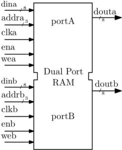
Fig. 4: Dual Port RAM
The dual port memories have separate control line for both the ports. The various modes of a typical true dual port RAM are shown below. In the mode 1, writing of data is possible through both the ports but not on the same location. In mode 3, data can be read through both the ports even from the same address location. In mode 2 and 3, one port is busy in writing while another port is reading data.
Table 1: Modes of Dual Port RAM
| modes | ena | wea | enb | web | portA |
portB |
| 1 | 1 | 1 | 1 | 1 | write | write |
| 2 | 1 | 1 | 1 | 0 | write | read |
| 3 | 1 | 0 | 1 | 1 | read | write |
| 4 | 1 | 0 | 1 | 0 | read | read |
module dp_ram(clka,clkb,ada,adb,ina,inb,ena,enb,wea,web,outa,outb);

input clka,clkb,ena,wea,enb,web;

input[2:0] ada,adb;

input[7:0] ina,inb;

output reg [7:0] outa,outb;

reg [7:0] mem [0:7];

initial begin

outa = 8'b00000000;

outb = 8'b00000000;

end

always@(posedge clka)

if(ena)begin

if(wea)

mem[ada]=ina;

else

outa = mem[ada];

end

else

outa = outa;

always@(posedge clkb)

if(enb)begin

if(web)

mem[adb]=inb;

else

outb = mem[adb];

end

else

outb = outb;

endmodule
Similarly Dual Port ROM is also possible. The simple block diagram of a Dual Port ROM is
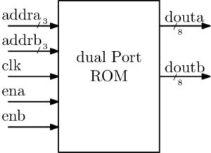
Fig. 5: Dual Port ROM
Realization of higher memory blocks
Higher capacity memory blocks can be realized using low capacity memory blocks by cascading. Realization of a 32×8 ROM using 8×8 memory block is shown below.
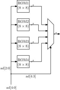
Fig. 6: Realization 32×8 ROM using 8×8 ROM (4 numbers)
Go to the Top
Simple Dual Port RAM
A general question arises in mind that how the dual port RAMs are realized. A conceptual diagram of a simple Dual Port RAM having only 4-bit memory is shown below.
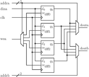
Fig. 7: Conceptual Diagram of a Simple Dual Port RAM
In a true Dual Port RAM, writing can be done through both the ports. Also, it has the separate clock, en and we signal for separate ports. In case of simple Dual Port RAM writing is done through port A and reading can be done through both the ports.
Note:
- For storing constant data, ROM should be used.
- A dual port ROM is preferred over two single port ROMs.
- Always use enable inputs to disable the memory blocks when not in use.
*More on memory blocks will be discussed in the post on FPGA implementation of digital systems.
Click here to download the file
Memory Initialization
One method of memory initialization is shown above for ROM, which is by assign statement. But for bigger memory size it is very difficult to initialize this way. Another way is
 initial begin
 $readmemb("c1.txt", mem);
 end
Here the readmemb command loads the memory array from a text file c1.txt. Here in the text file data are written in binary. To load the data in hexadecimal format the command readmemh can be used.
The intellectual property blocks provides easy initialization by .coe files. The data written in .coe file can be loaded to the memory arrays easily.
How can I help you. Be specific.
I was suggested this web site by way of my cousin. I am not sure whether this publish is written by him as nobody else understand such precise approximately my difficulty. You’re wonderful! Thank you!