In the previous three tutorials, we have learned how prepare the files which are needed to start the placement and routing using INNOVUS. In this tutorial, a basic tutorial on how to perform placement and routing using INNOVUS is given. This is a very fundamental and only covers the basic ideas and follows the tutorial provided by the CADENCE. If any one interested in more details then they are advised to go through the full CADENCE manual on the INNOVUS.
Step by step Placement and Routing with INNOVUS
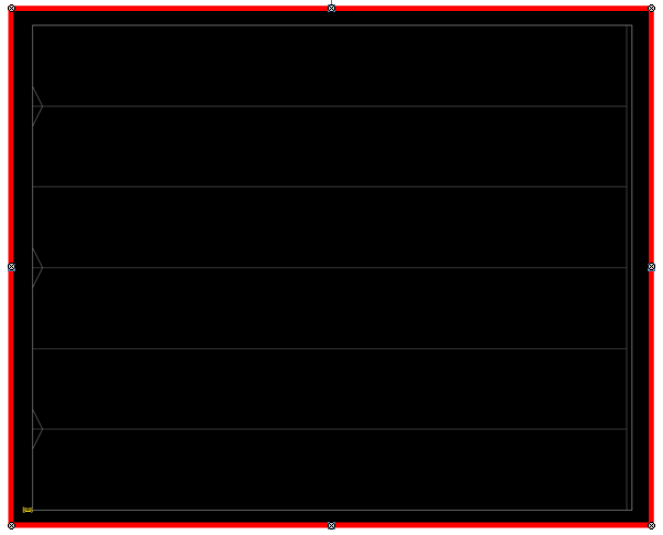
Step 1 – File Import (Can be found in tutorial on design and file import). Once all the files are imported the first window that appears to us is shown below.
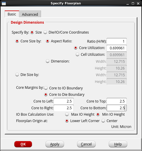
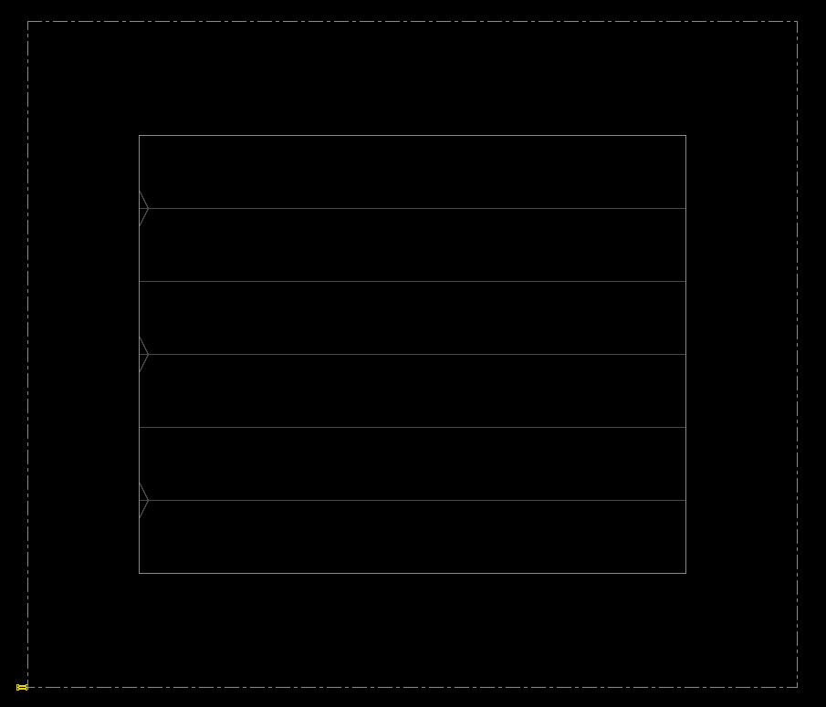
Step2 – Choose Floorplan – Specify Floorplan
Tool automatically gives a floorplan using Core utilization factor. Here, Core to die distance is mentioned but core to IO boundary also can be mentioned here. In this case, IO pad length must be taken into account. Lets say Core to die distance = 10 for core area of  . The size of the chip is
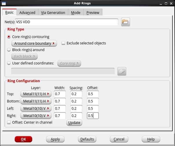
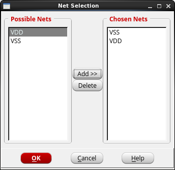
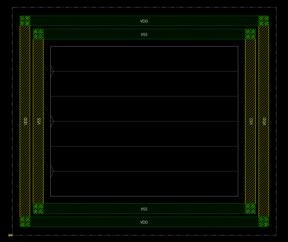
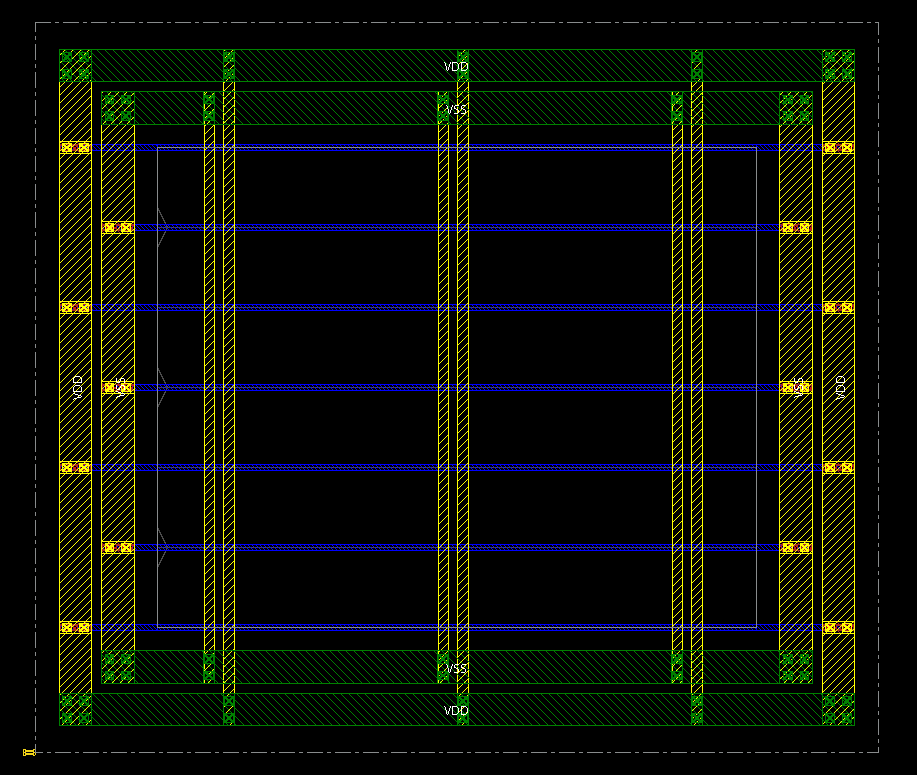
Step 3 – Choose Power-Power Planning ‒ Add Ring.
Power Rings carry VDD and VSS around the Core. First choose the power nets. In our case it is VDD and VSS. There are four Metal rings in our case. The Metal layers are used as
Bottom – Metal 3 (M3), Top – Metal 3 (M3), Right-TOP Metal (TOP_M), Left-TOP Metal (TOP_M)
Width = 2, Spacing = 1, offset = 2.5 (2.5 + 2 + 1 +2 +2.5 = 10)
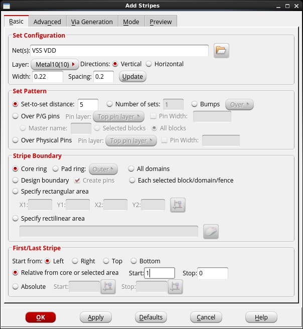
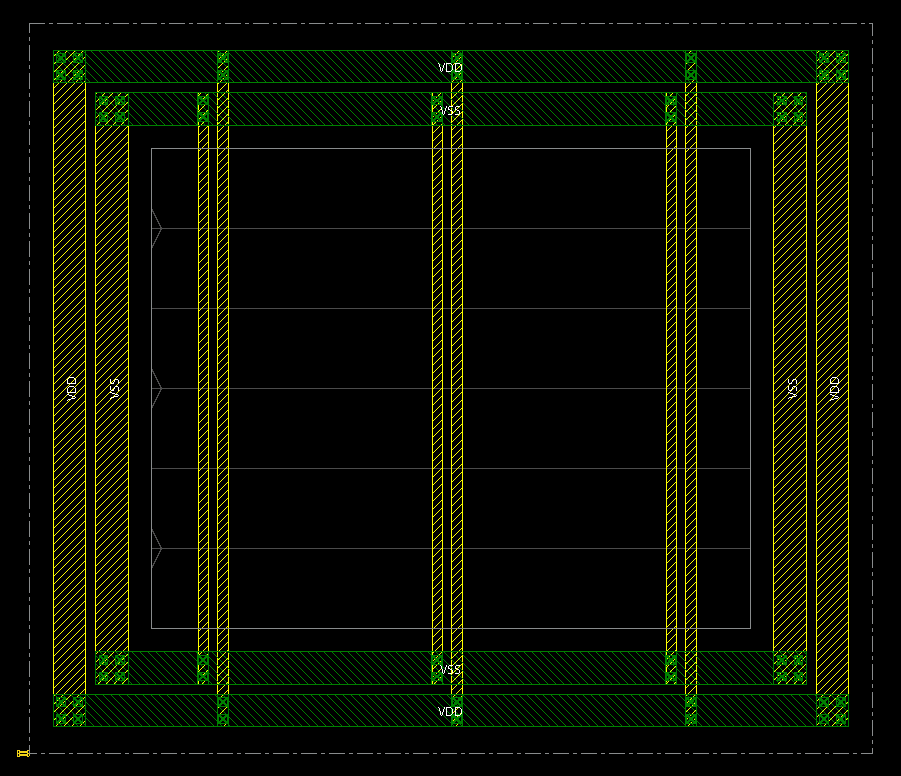
Step 4- Choose Power-Power Planning ‒ Add Stripe. The Add Stripes form appears.
Stripes connect the power nets through the Core are. They can be vertical or horizontal. Choose Top Metal as they are Vertical here. A set is combination of VDD and VSS. Width = 2 and spacing between the nets is 1. The set to set distance is 20 and there will be 18 sets.
480 = 15 + (20+5)18 + 15 here 15 is the relative distance from the core area.
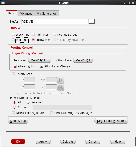
Step 5- Choose Route ‒ Special Route.
Special Routes connects the Power nets t the standard cells. Here, retain all the options as it is in the image. Only select Metal 1 as the bottom layer and TOP Metal as Top layer
Step 6 – In creating Rings, Strips and SRoutes make sure that the vias are created correctly. If not then must be started from the beginning.
Step 7- Scan Definition
The following command will load the SCANDEF file that was created during synthesis pocess.
defIn counter.scandef
setScanReorderMode –compLogic true
setPlaceMode –place_global_place_io_pins true
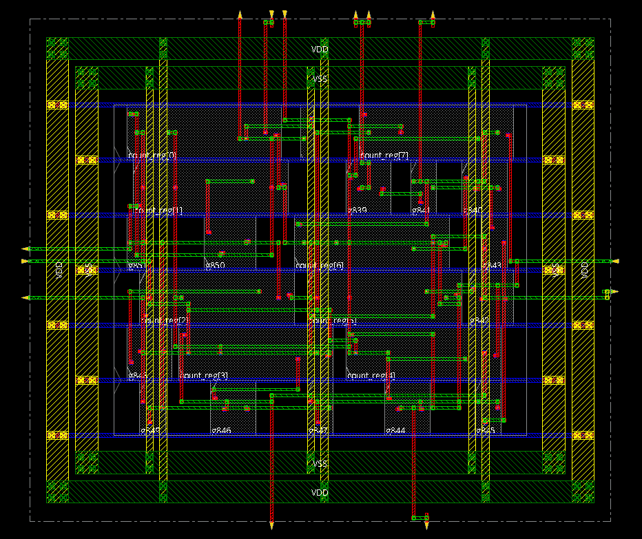
Step 8- Placement of Standard Cells…..without any optimization……
setPlaceMode -fp false
#setPlaceMode -placeIoPins true
placeDesign -noPrePlaceOpt
#place_opt_design —– Optimization during placement can also be done.
Step -9 Clock Tree Synthesis
Clock tree Synthesis is done without any specification file. The following file creates the specification file from the SDC file.
create_ccopt_clock_tree_spec
The following command is universal command for the clock tree synthesis. This command not only synthesizes the clock tree but also optimizes it by placing buffers.
ccopt_design
Step 10 -Post CTS Optimization…..
timeDesign -postCTS
optDesign -postCTS
timeDesign –postCTS
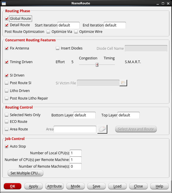
Step 11 – Routing
choose Route – NanoRoute – Route. The NanoRouteform is displayed.
Step 12- Post Route Analysis…….
setAnalysisMode -analysisType onChipVariation
timeDesign -postRoute
#optional when there is any violation….
optDesign -postRoute –hold
timeDesign -postRoute
report_timing
Step 13- Add Filler Cells – There various type of metal fillers available in library.
Step 14 – Physical Verification
Choose Verify – Verify Geometry
Choose Verify – Verify DRC
Choose Verify – Verify Connectivity.
Choose Verify – Verify Antenna
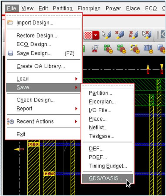
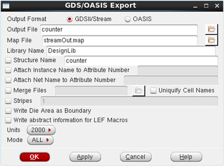
Step 15 – GDSII file extraction: Follow the steps shown in the following image.
Give output file name as counter.gds. One important thing is not shown here which merging technology GDS files. The counter.gds file should be merged with technology GDS files which are tsl18fs120.gds and tsl18cio250_4lm.gds
Step 16- This GDS file can now be imported to CADENCE Virtuoso for extracting the layout and further analysis. Also can be used for mixed signal layouts.
The tutorial may not be flawless but enough to give the readers idea about Placement and Routing using INNOVUS.
Thank you very much for the detaled explanation….
Thank you for visiting……