Interfacing ADC with FPGA board is important when we need to acquire an analog signal to process it in FPGA. In many academic projects we are asked to demonstrate the real time application of a digital system implemented on FPGA. In doing that, we find it difficult to interface an ADC chip with FPGA as a separate HDL code is required to write. In this blog, a tutorial on interfacing ADC with FPGA is given. Here, we have chosen an ADC chip to interface with FPGA board which can be applicable to other chips also.
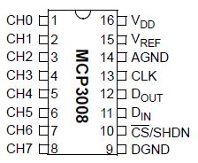
The selected ADC chip (MCP3008) is a product of Microchip Company. It is a 10-bit ADC chip having 8 input channels. It is capable of sampling at 200 ksps at VDD of 5.5 V. Minimum clock frequency is  . More details about the ADC chip can be found in the specification document of the chip.
The pin diagram of the chip is shown in Figure 1.
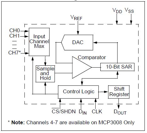
The ADC inside the chip is SAR logic based. It has 8 channels and input can be selected through any channel. The basic functional diagram is shown in Figure 2.
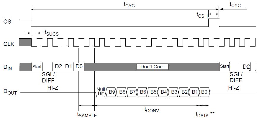
Nowadays every chip is either SPI or I2C protocol based. The chip we are considering here is SPI based. The shift register outputs data serially through the pin  . It has a CLK pin at which frequency should be kept at 18 times higher than the sampling frequency. The pin
  is for controlling the SAR logic of the ADC and it is an active low signal. The serial pin
  provides the control word. The timing diagram is shown in Figure 3.
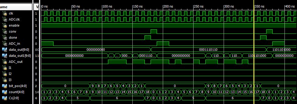
The SPI protocol based ADC chip is interfaced with FPGA by writing a Verilog code. The Verilog code written here is FSM based as we are less concerned about the performance of the code. IN that we have defined separate states for every status on the pin. The code receives the output data and make a valid word. The start bit is kept high and the next bit defines how we take analog signals. If it is high then it is single ended and if low then it is differential. The next three bits are for selecting input channels. The SPI based controlling of the ADC chip is shown in Figure 4.
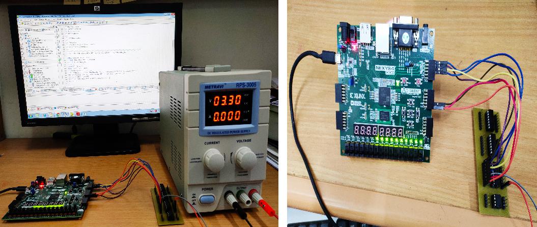
To demonstrate that the ADC chip is interfaced with FPGA, we haven chosen NEXYS 4 DDR board. The ADC chip is mounted on a PCB along with other chips. We have taken a DC voltage source to feed analog input to the ADC chip. We have varied the voltage source from 0 to 3.3 volt which is maximum voltage of the FPGA board. The experimental setup is shown in Figure 5. Here we can see that all the 10 LEDs are blinking when voltage is 3.3.
The formula for interpreting the digital value from an 10-bit ADC chip is

Click here to download the Verilog code.
Hi,
I have seen your project, can you send the wiring of FPGA to MCP3008.
Hey Hi,
It is such a nice article and was very helpful.
Can you please send the circuit wiring of FPGA to ADC (pin connections between ADC and FPGA)
Thank you 🙂
I think it is given…or u can refer the ADC datasheet.