I. Introduction
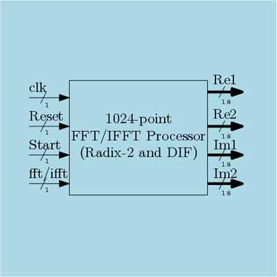
Fast Fourier transform (FFT), an efficient technique to perform discrete Fourier transform (DFT), is the most important block in the signal processing domain. FFT is used to convert a signal in time domain to its frequency domain. On the other hand, inverse FFT (IFFT) block is used to convert the signal in frequency domain to time domain. The evaluation technique of FFT and IFFT is very similar and thus it is required to perform both the operations by a single processor. In this work, an Efficient FPGA Implementation of 1024-point FFT/IFFT Processor is reported.
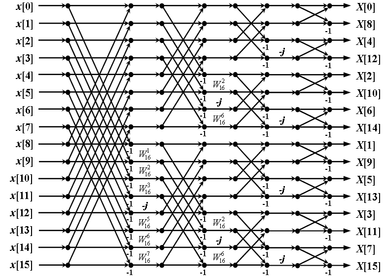
In our previous work, 8-point FFT architecture was implemented. In this work, a 1024-point FFT/IFFT processor is designed. This processor is designed such a way that it can perform FFT and IFFT based on a control signal  . This processor is based on Radix-2 decimation in frequency (DIF) technique to implement FFT algorithm. In this design, the input samples are in order but the output samples are not in order. Signal flow diagram for a basic 16-point Radix-2 FFT is shown in Figure 1.
Find MATLAB Realization of FFT/IFFT w/o Direct Function Here
In an N-point FFT block, n is used to represent the number of stages where  . In this signal flow diagram shown above, there are
  stages and it can be seen that the input samples are in order. Similar way, in case of 1024-point FFT there will be total 10 stages. In this work, a fully parallel and also pipelined design for 1024-point FFT/IFFT processor is presented. This processor is hardware efficient, fast and also storage efficient.
II. Architecture of 1024-point FFT/IFFT Processor
The FFT/IFFT processor data path is shown in Figure 2. All the stages from stage 1 to stage 2 are identical but stage 9 and stage 10 are different. The only difference between stage 1 and stage 2 is that mux unit (MU) is not present in case of stage 1. The processing element (PE) block is same in stage 1 to stage 8. FFT operation is performed when signal is high and IFFT operation is performed when signal is low. The  control signal is used to invert the elements of memory buffer (M) when required. The memory buffers denoted by ‘M’ are used to store the twiddle factors. The size of the memory buffers for twiddle factor varies stage wise. Maximum size is used for stage 1 and minimum size is used for stage 8. Phase input (
 ) and phase output (
 ) are the control signals to select the elements from the MU.
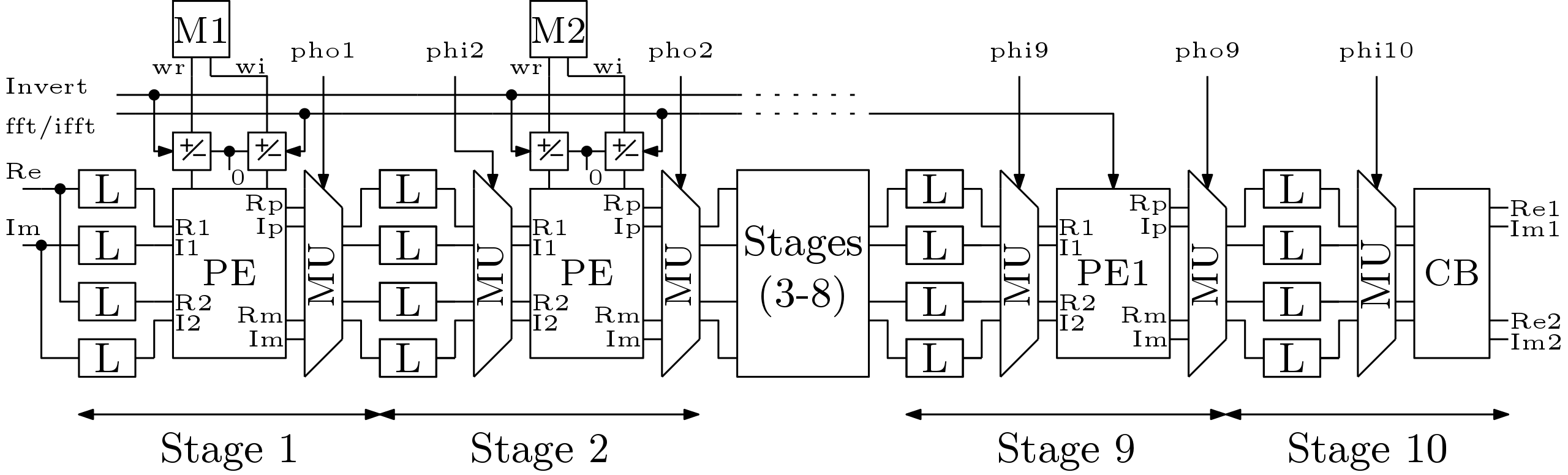
In stage 1, input samples from the external world or from any design are fed to a memory block. In the memory block, ‘L’ indicates line buffer. Two line buffers are there for real samples and two line buffers are for the imaginary part. Initially samples are written to the top line buffer and then the samples are written to the bottom line buffer. This way half of the samples are written in the line buffers at top position and half of the samples are written to the line buffers at bottom. This way the samples are acquired. The sizes of the line buffers are same throughout the architecture.
The operation FFT/IFFT block is straight forward and this processor is twiddle factor storage based. This means twiddle factors are stored instead of generating them using CORDIC type block. The throughput of this processor is 2. This means two complex data are outputs per clock sample. The details of the sub blocks are explained below.
1. Processing Element for 1024-point FFT/IFFT Processor
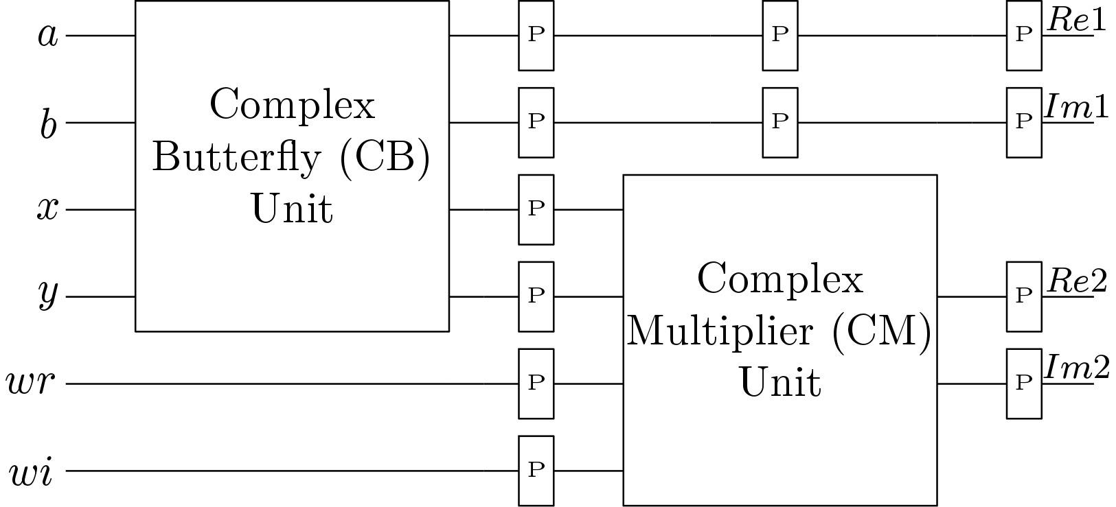
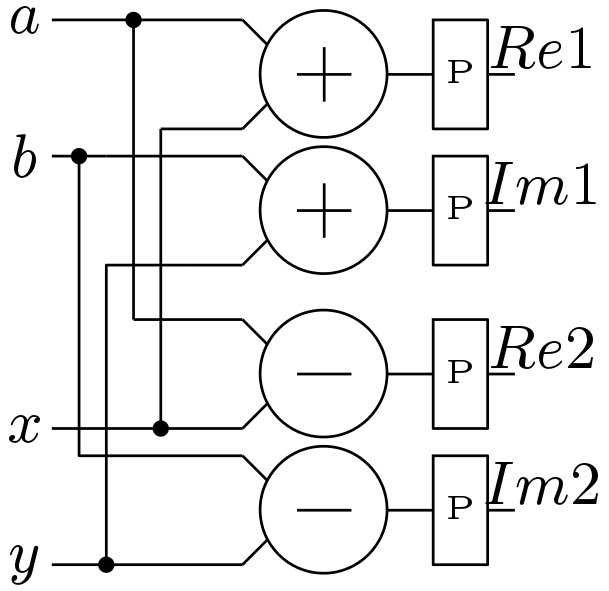
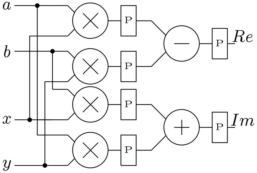
Processing element is the major part of any stage of the processor. This block is mainly responsible for the complex arithmetic operations. The block diagram of the processing element (PE) is shown in Figure 3. The PE block consists of a complex multiplier (CM) block and a complex butterfly (CB) blocks. All the necessary pipeline registers are inserted at suitable positions. The block diagram of the CB block is shown in Figure 4. A simple block diagram of the CB block is used here which has two adders and two subtracters. The schematic of the CM block is shown in Figure 5. CM block is also based on the simple circuit and no efforts have been made to optimize it. Though there is a low power version of the CM block is available, this simple block is used here. This block needs one extra multiplier compared to the low power version.
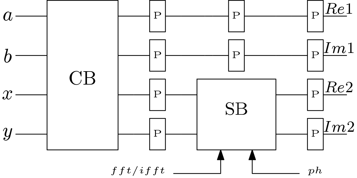
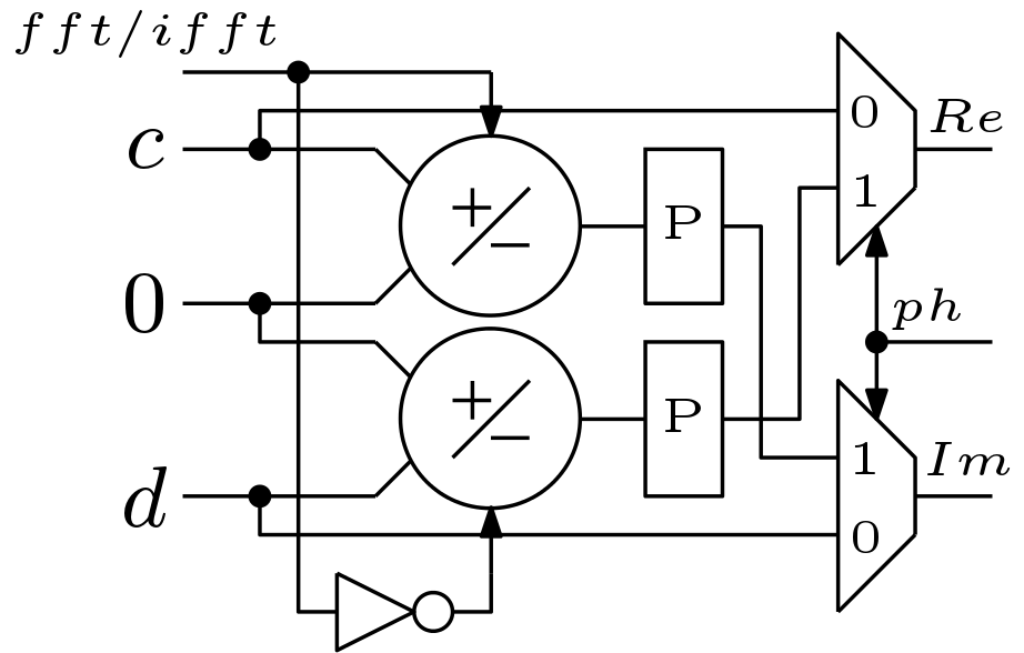
The processing element 1 (PE1) block is different and hardware efficient than the previously discussed PE block. This is because no multiplication is required in the 9th stage. Only controlled inversion of the input data is enough. The schematic of the PE2 block is shown in Figure 6. Here, CB block is same as it was for PE block. But the CM block is replaced with a hardware efficient sub block (SB). The schematic of the SB block is shown in Figure 7. SB block consists of two add/sub blocks and two multiplexers. The add/sub blocks are used for inversion depending on the control signal . The  signal selects from the multiplexers. The frequency of the signal is half of the frequency of the clock signal.
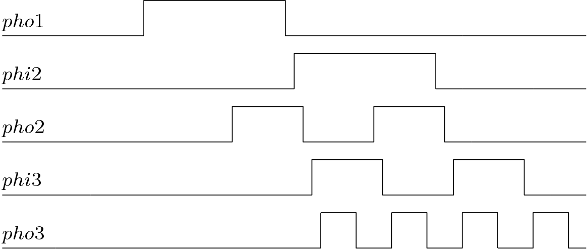
2. Multiplexer Unit
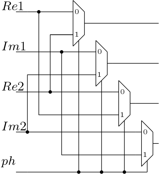
The MU block selects the samples which are output of the processing elements or the line buffers. The schematic of the MU is shown below in Figure 8. This MU blocks have control signal or depending on the position of the MU blocks. The phase diagrams for the or signals are shown in the Figure 9.
3. Twiddle Factor Multiplication
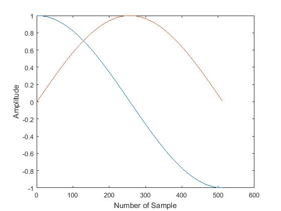
Twiddle factors are stored in the memory elements. These memory elements are denoted as M1, M2 and so on. Each row or each column of the twiddle factor matrix is basically a complex sinusoidal atom. The real value of an atom is a cosine pulse and the imaginary part is a sinusoidal pulse. Frequency of the first atom is half the frequency of the 2nd one. Similarly frequency of the 2nd atom is half the frequency of the 3rd one. This way the last atom has the highest frequency.
A sinusoidal pulse can be achieved by shifting a cosine pulse by 90 degree and by suitable sign change. This is why it is not required to store both sine and cosine pulses. Thus only cosine pulse is stored and lots of memory storage elements are saved. The cosine pulse can be divided into two symmetric halves. Further memory storage reduction is achieved by storing only one part out of the two parts of a cosine pulse. This is shown by the Figure 10.
4. Storing of Intermediate Data Samples
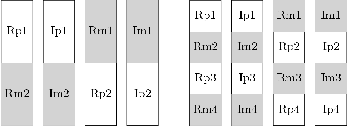
Size of the line buffers in all the stages are same but storing technique is not same. Output of the first processing block in the first stage has four outputs. Two real parts (Rp and Rm) and two imaginary parts (Ip and Im). Suffix ‘p’ represents the outputs which are resulted by addition. In the line buffers, the value of Rp and Rm is stored alternatively as it is shown in Figure 11. In case of first line buffer, Rp1 is stored in the first halve and Rm2 is stored in the 2nd halve. But in the 3rd line buffer, Rm1 is stored in the first halve and Rp2 is stored in the 2nd halve. Similarly the imaginary values are stored 2nd and 4th buffer. This way the output of the 2nd processing block is stored in the line buffers but this time total memory space is divided into 4 sections. Storing technique for the 2nd stage is shown also in Figure 11 (right side).
II. Performance Analysis of 1024-point FFT/IFFT Processor
In this work, a 1024-point FFT/IFFT processor is designed and this processor performs both FFT and IFFT based on a control signal. Performance analysis is carried out here in terms of hardware, speed and power consumption. The pipelined operation of the N-point FFT/IFFT processor is shown in Figure 12 for up to 5 stages. Here, each stage of the FFT/IFFT processor has some latency. The first stage has latency of  clock cycles. It can be said that the total latency of this processor for
  is (1023 + 10) = 1033 clock cycles. This way the timing complexity of the processor can be calculated and this is
  clock cycles.
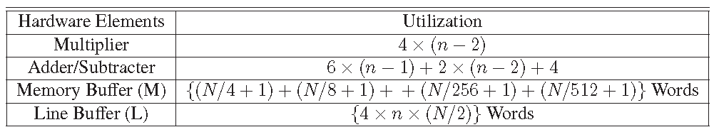
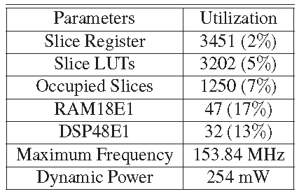
Hardware complexity is another parameter which is also should be analyzed to measure the performance of this processor. Resources utilization of the processor is shown in Table 1. The Verilog implementation of the processor is targeted to the XC7A100T-2CSG324 FPGA module. The FPGA implementation performance of the processor is shown in Table 2. The architecture is designed and validated using 18-bit fixed representation, where 8-bits are used for integer part and 10-bits are used for fractional part.
IV. Conclusion
In this work, FPGA Implementation of 1024-point FFT/IFFT Processor is presented and implemented on FPGA platform and performance of this implementation is analyzed in terms of parameters like hardware complexity and timing complexity. The FFT/IFFT processor is based on Radix-2 DIF technique based and architecture is parallel with pipeline stages. The objective of this implementation is to reduce the storage requirement to store the twiddle factors. The processor is efficient and scalable to value of  . Further optimization can be done in this processor by optimizing the processing element block but not done in this work to keep the architecture simple.
Verilog Code of 1024-point FFT/IFFT Processor
Specifications:
- 1024-point FFT/IFFT processor is implemented.
- Architecture is based on Radix-2 DIF algorithm.
- Throughput – 2 complex data per clock cycle.
- Latency – 1033 clock cycles.
- Design is targeted to XC7A100T FPGA device.
- 18-bit data width is used.
- Maximum frequency – 153.84 MHz.
Click here to find the detail specifications.
There seems to be a typo at figure 3. Second block should be Complex Multiplier (CM) unit, while there it is captioned Complex Butterfly (CM) unit.
I am not seeing any typo mistake.. In figure 3 first block CB and second block is CM.
Yes you are correct. There is a typo.. Which I should corect..