Previously we have discussed clock division by odd and even numbers in the tutorial sequential circuits. Later we have also developed a programmable clock divider that divides clock frequency by any integer from 1 to 15. This tutorial talks about clock division by non-integers which is also required is some critical digital systems.
Clock division by integers generates clock signal of 50% duty cycle but in case of non-integers duty cycle can not be 50%. Only analog Phase-Locked Loop (PLL) circuits can achieve clock division by non-integers with 50% duty cycle. In this tutorial we will discuss clock division by non-integers according to the circuits reported in [1]. Three types of schemes are discussed here.
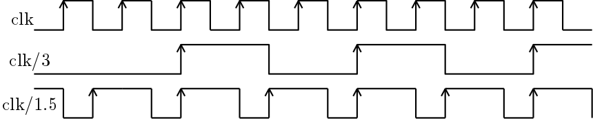
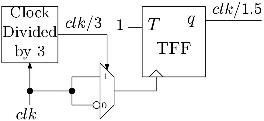
Scheme 1: Clock division by 1.5
Here, Figure 1 shows the division of clock frequency by 1.5. The signal clock divided by 1.5 is generated by clock divided by 3 signal. Clock division by 3 can be achieved by any scheme mentioned in sequential circuits. The scheme for clock division by 1.5 is shown in Figure 2. Here duty cycle is 66.66% instead of 50%. Glitches can be generated in this scheme of clock division due to the presence of the MUX.
Scheme 2: Clock division by 4.5
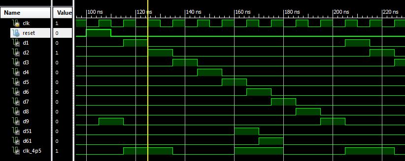
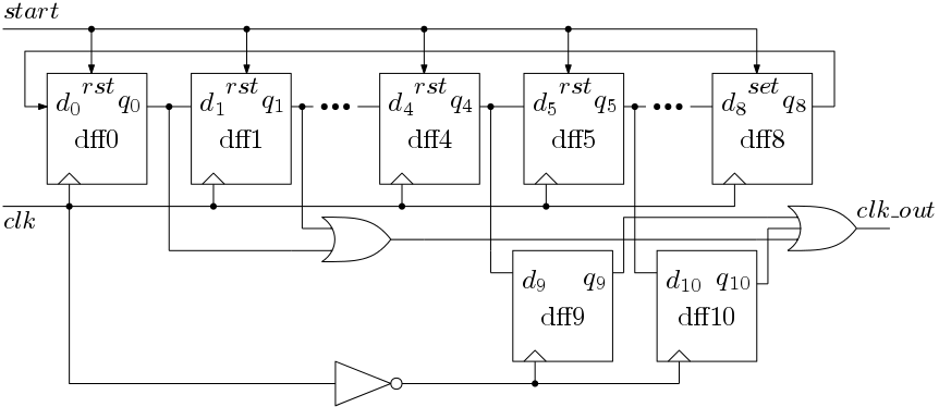
Shift register based clock division schemes are also possible. In order to divide the clock frequency by 4.5, a 9-bit Serial Input Serial Output (SISO) is taken. Initially, flip-flops are loaded with 000000001. This means the 9th flip-flop is set and others are cleared. Output of the 9th flip-flop is fed to input of the first flip-flop. The phase signals are shown in Figure 3. This scheme is shown in Figure 4. Output of the first and second flip-flop are ORed to divide clock by 4.5. Also output of the fifth and sixth flip-flop is delayed by half-cycles and then ORed. The result of these two OR operation is then ORed to generate the output signal. Here start signal sets the 9th flip-flop but clears all other flip-flops. Here, dff9 and dff10 are negative edge triggered. Duty cycle is 44.44% instead of 50%. This scheme is glitch free compared to scheme 1.
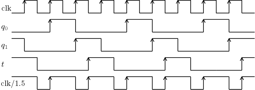
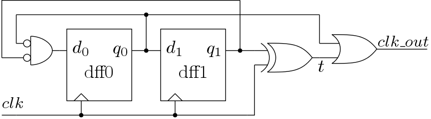
Scheme 2: Clock division by 1.5
Another approach for clock division is LUT based. The phase diagram for clock division process is shown in Figure 5. Here,  and
and  are both result of clock division by 3 but they do not have 50% duty cycle. These signals together with clock signal generates the desired clock signal.
The signal  is generated by ORing and signal
  . Keeping the signal fixed we need to generate signal using clk and . Table 1 shows the truth table generation of signal .
| clk | | |
| 0 | 0 | 0 |
| 0 | 1 | 1 |
| 1 | 0 | 1 |
| 1 | 1 | 0 |
.The scheme for clock division by 1.5 by LUT approach is shown in Figure 6. These scheme has two parts and first part is the circuit for clock division by 3. Second part is required to generate signal and output signal.
Similarly we can develop circuit to divide clock frequency by 2.5 using LUT approach. The Verilog code for clock division by 2.5 is given in the downloadable Verilog file.
Verilog code for clock division by 1.5, 2.5 and 4.5 (6898 downloads )[1]. Mohit Arora, “Clock Dividers Made Easy”, Design Flow and Reuse (CR&D), ST Microelectronics Ltd, Plot No. 2 & 3, Sector 16A, Noida-201301, India
This vlogs are very useful.How to build a programmable clock divider for fractional number.
This vlogs are very helpful.How to design a programmable clock divider for fractional numbers?