The impulse response of a Finite Impulse Response (FIR) filter is of finite duration as it settles to zero in finite time. In comparison to the Infinite Impulse Response (IIR) filters, there is no feedback in FIR filter. This feature makes the FIR filter always stable. Another important feature of FIR filter is that it can produce linear phases and thus in application where linear phase should be used, FIR filters must be preferred. Implementation of FIR filters is also straightforward compare to the design of IIR filters.
The FPGA manufacturing companies have provided many advanced features for rapid prototyping of the FIR filters. The advanced DSP blocks can perform many mathematical functions with greater speed. Thus implementation of FIR filters is no longer a critical job. The objective of this work to cover the aspects of implementation of FIR filters. In this work, FPGA implementation of a low pass FIR filter using different structures is presented. This filter is implemented with or without the advanced DSP blocks. Performance of all the structures is also compared in terms of resource utilization, latency and maximum frequency.
1. FIR Low Pass Filter
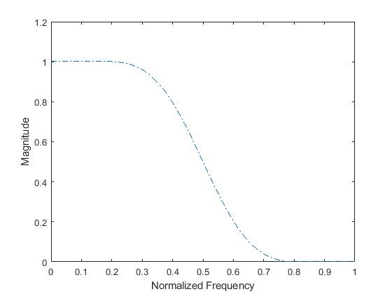
The frequency response of the low pass filter is
![\[ H(e^{jw})= \begin{cases} 1 & \text{for}\hspace{2pt} -\frac{\pi}{2}\leq w \leq \frac{\pi}{2} \\ 0 & \text{for}\hspace{2pt} -\frac{\pi}{2}\leq |w| \leq \pi \end{cases} \]](https://digitalsystemdesign.in/wp-content/ql-cache/quicklatex.com-ebd759f871e4f26c04fd1dd44579a0d5_l3.png "Rendered by QuickLaTeX.com")
Here,  is the normalized frequency and
  denotes the cutoff frequency in radian. This ideal low pass FIR filter can be realized using many techniques. Here Hamming window based design is followed. The transfer function
  of a N tap FIR filter can be written as
![\[H(z) = \sum^{N-1}_{n=0}c_nz^{-n}\]](https://digitalsystemdesign.in/wp-content/ql-cache/quicklatex.com-b0a206461cdaa5843e95e6c13b500574_l3.png "Rendered by QuickLaTeX.com")
Here, N can be both even or odd. The time domain expression of the low pass FIR filter is shown below for N=13.
![\[y = x.(c_0 + c_1.z^{-1}+ c_2.z^{-2}+c_3.z^{-3}+c_4.z^{-4}+....+c_{12}.z^{-12})\]](https://digitalsystemdesign.in/wp-content/ql-cache/quicklatex.com-76cbebc766bd9653a4c8d2c425b70c3a_l3.png "Rendered by QuickLaTeX.com")
The frequency response is shown in Figure 1
Click here to download the MATLAB code
2. Advanced DSP Blocks
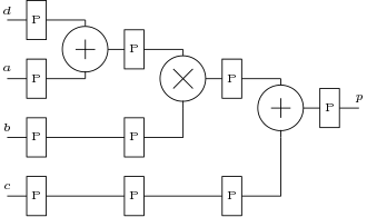
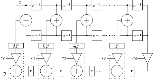
A basic structure of a DSP block is shown in Figure 2 to perform the operations which are useful in realizing FIR filters. The DSP block includes a pre-adder, a multiplier and an ALU. The ALU can be used to realize various functions but here ALU performs only addition or subtraction. The DSP block has a  input and based on the status on this line the DSP block performs many different functions. For example, the DSP block shown here can evaluate
  or
or  . The pipeline registers are programmable, means they can be inserted or removed or increased. This DSP blocks are inbuilt and thus provides faster speed than the implementations using the LUTs.
3. Different Filter Structures
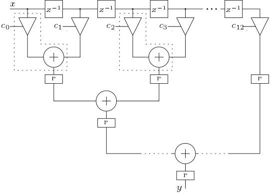
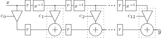
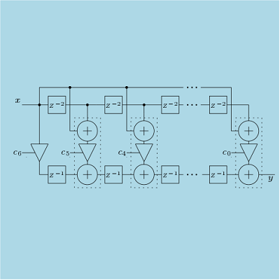
3.1 Direct Form Structure
Direct form structures directly implements the FIR transfer functions. Direct form 1 structure (Figure 3) is the most direct implementation of FIR filters. It uses an adder tree to add all the outputs of the multipliers. Direct form 2 structure (Figure 5) is the systolic architecture. Here pipeline registers are inserted to achieve maximum frequency. Direct form 3 structure (Figure 5) is the transposed structure which do not need the pipeline registers.
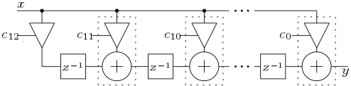
3.2 Linear Phase Structures
If the co-efficients of the transfer function are symmetric in nature then the linear phase can be achieved. The transfer function of the low pass filter can be written as

The basic linear form 1 structure (Figure 6) consumes almost half multipliers than that is used for direct implementations. The linear form 2 structure (Figure 7) is a transposed architecture and uses less pipeline registers. But it has higher combinational path. The linear form 3 architecture is developed using the DSP block which achives higher maximum frequency.
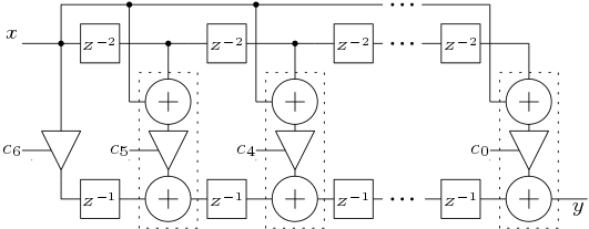
3.3 Polyphase Structures
The transfer function of a FIR filter can be written as summation of two terms where a term contains all the even indexed co-effcients and the other term contains odd indexed co-efficients. The transfer function of the low pass filter can be expressed as
![\[ H(z) = (c_0 + c_{2}z^{-2} + c_{4}z^{-4} + ... +c_{12}z^{-12}) + (c_1 z^{-1} + c_3 z^{-3} + ... +c_{11}z^{-11})\]](https://digitalsystemdesign.in/wp-content/ql-cache/quicklatex.com-f6941ce6fb973eff7a7be1497482c876_l3.png "Rendered by QuickLaTeX.com")
This equation can also be written as
This is equal to
![\[ H(z) = (c_0 + c_2z^{-2} + c_4z^{-4} + ... +c_{12}z^{-12}) + z^{-1}(c_1 + c_3z^{-2} + ... +c_{11}z^{-10}) \]](https://digitalsystemdesign.in/wp-content/ql-cache/quicklatex.com-2328b562a023a5f78546414a02d07608_l3.png "Rendered by QuickLaTeX.com")
![\[ H(z) = P_0(z^2) + z^{-1}P_1(z^2) \]](https://digitalsystemdesign.in/wp-content/ql-cache/quicklatex.com-d6b3501d67deb47a43c246aeb50a4635_l3.png "Rendered by QuickLaTeX.com")
Two Polyphase structures are designed here. One is Polyphase structure 1 (Figure 8) which directly implements the filter. Other is Polyphase structure 2 (Figure 9) which is implemented by sharing the delay elements.

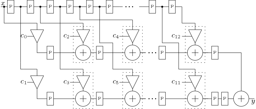
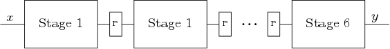
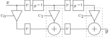
3.4 Cascaded Structure
In the cascaded form, the higher order transfer function is realized by cascading lower order FIR sections where each section realizes either a first order or second order transfer function. The cascaded form structure of the FIR low pass filter is shown Figure 10. The second order sub-block is shown in Figure 11.
4. Performance Estimation
4.1 Implementation Issues
The following things must be taken care to design an efficient architecture of FIR filter.
- Architecture: In this work all the parallel architectures are discussed. But higher order FIR filters consume higher resources. Thus serial architecture or architecture folding can be adopted. Pipeline registers are important to achieve higher maximum frequency.
- Data Format: The FIR filters suffer from the quantization error. The quantization error depends on firstly on the data format. There are two formats, floating point and fixed point. It is obvious that floating point format gives better accuracy but uses more hardware. The fixed point format is preferred here and the word length controls the quantization error. The word length should be chosen in such a way that minimum resources are used with acceptable accuracy.
- Constant Multipliers: The major block is the multiplier which multiplies the input signal by the known constants. Thus constant multipliers can be used in place of complete multipliers. The constant multipliers multiply a constant using add and shift method. This customization of multipliers can be useful in case ASIC implementation but in case of FPGA implementation the DSP blocks blocks are designed optimize according to the multiplicands.
5.2 Design Performance
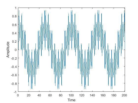
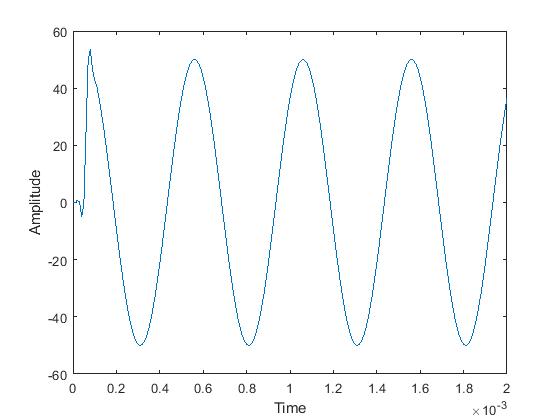
In this work, 13-tap low pass FIR filter is implemented on NEXYS DDR2 artix7 FPGA device (xc7a100t-3csg324). The low pass filter is verified by taking two sinusoidal signals of frequencies 22 KHz and 20 KHz. These two signals are multiplied and output of the multiplier is given to the low pass filter. The sampling frequency is taken as 100 KHz and thus the low pass filter filters out the signals whose frequency greater than 25 KHz. The output of the filter is a tone of 2 KHz which is shown in Figure 12. The original output signal obtained from MATLAB and the FPGA based filtered output is compared in Figure 12. Here, 20-bit fixed point data width is chosen for implementation where 12-bit is reserved for fractional part. Here, Root Mean Squared Error (RMSE) is used to measure the design performance. RMSE is computed as
![\[RMSE = \frac{{\left\lVert(\hat{y}-y)\right\rVert}_2}{{\left\lVert y \right\rVert}_2}\]](https://digitalsystemdesign.in/wp-content/ql-cache/quicklatex.com-b2a55082b8fd5e401db107e03f6fc123_l3.png "Rendered by QuickLaTeX.com")
Here y is MATLAB based filtered output and  is FPGA output. A RMSE of 0.0006728 is achieved using 20-bits of word length.
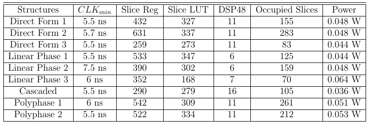
5.3 Comparison
Comparison of the implementation of the different structures is shown in Table 1. The dynamic power is computed at the maximum achieved frequency. It is clear that transposed direct form architecture is better than the other direct form structures as it do not consume pipeline registers. The linear phase structures can only be used when the co-efficients are symmetrical. Linear phase 2 architecture achieves less frequency as it has a long critical path. But Linear phase 3 architecture implements same linear phase 2 structure but with DSP blocks. Here, higher maximum frequency is achieved and also other resources are are less used with higher power consumption.
Click here to download the article in PDF.
Click here to download the input file for the Verilog Files.
Verilog Code for Different FIR Low Pass Filters
FPGA implementation of FIR filters is very common topic for signal processing or VLSI engineers. FIR filters have many applications in implementations of any real time systems. Here, we have provided Verilog codes for different FIR low pass filters. These configurations are Direct form 1 and 2, Cascaded form, Linear Phase form and Polyphase form. A Matlab code is also associated.
16 (Downloads)