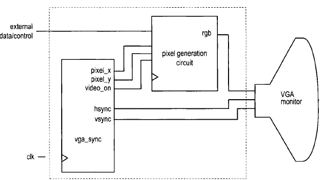
A video controller generates the synchronization signals and outputs data pixels serially through the VGA port of the FPGA board. The synchronization signals generator circuit (vga_sync) generates the timing and control signals. The hsync and vsync signals control the horizontal and vertical scans. The pixel_x and pixel_y signals specify the current location of the pixel. The vga_sync circuit generates the video_on signal to indicate whether to enable or disable the display. The Pixel generation circuit generates the three video signals which are collectively referred to as the rgb signal.
VGA Signal Timing:
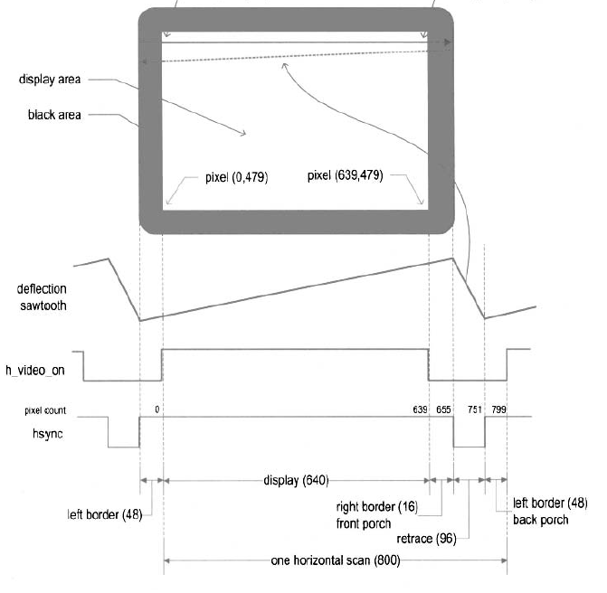
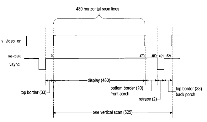
The following discussions are based on a 640-by-480 VGA screen.
The refresh rate for the display is fixed at 60 Hz, which is the typical value used in monitors. In order to achieve this refresh rate on a 640×480 pixel screen, the pixel rate calculation is done as follows:
Pixel Rate = (Total Horizontal Pixels * Total Vertical Lines *Number of screens / second)
= 800 * 525 * 60 = 25 MHz
HDL implementation of VGA Controller:
Implementation details:
- The sync signal can be obtained by a special mod-800 counter and a decoding circuit. We intentionally start the counting from the beginning of the display region so that the counter output can be used as the horizontal (x-axis) coordinate. This output constitutes the pixel_x signal.
- The vsync signal can be obtained by a special mod-525 counter and a decoding circuit. This output constitutes the pixel_y signal.
- video_on signal is used to indicate whether the current vertical coordinate is in the displayable region. It is asserted when the line count is smaller than 480.
- 50MHz board clock is used as the system clock.
- The pixel clock is half of the system clock. A mod-2 counter is used to generate 25MHz pixel clock signal.
- The pixel tick should be routed via port as output signal to pixel generation circuit to extract the pixel content at the same rate.
- The values of the various regions of the horizontal scans and vertical scans are defined by the constants.
- To avoid glitches, the output buffers are inserted for the hsync and vsync signals.
The interfacing details of FPGA for VGA:
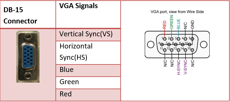
The Spartan 6 FPGA board that we used for this project has a built-in VGA port with 10 active signals as, hsync, vsync and video signals – 3bit(red), 3bit(green), 2bit(blue).
Click here to download the Verilog code.
Post Credit – Ardhendu Sarkar ( Junior Research Fellow, Computer Science & Technology, IIEST-Shibpur)
Great post.|