Previously many tutorials are published on how to design the basic building blocks of a complex digital system. In this tutorial, we are going to implement a digital system to demonstrate the techniques involved in implementing a system. Fast Fourier Transform (FFT) is a very popular transform technique used in many fields of signal processing. In this tutorial, we have chosen 8-point Decimation In Time (DIT) based FFT to implement as an example project. We have implemented 8-point FFT on Spartan 3E FPGA target and obtained its design performances. This design may not be directly useful, but the techniques involved in this project will help in implementing other complex projects.
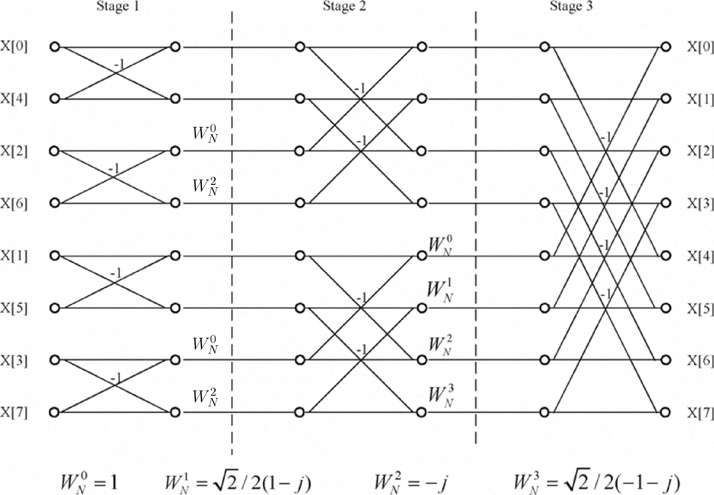
The basic signal flow diagram for 8-point DIT based FFT is shown below. In this case, input data samples are out of order but the output samples are in order. The different twiddle factors are also mentioned in that diagram. We will discuss the FPGA implementation without discussing any theory of FFT. For detailed theory of FFT any signal processing book can be refereed.
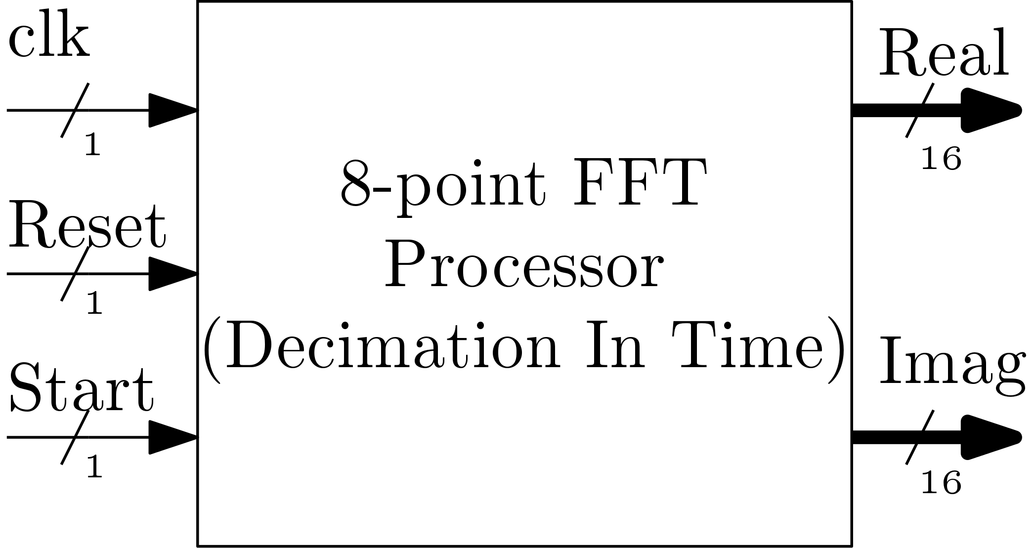
The FFT processor to be designed should have less number of input and outputs. The processor will have a clk pin, a reset pin and start pin as inputs. A pulse at the start pin will start the transform operation. The processor has two output vectors, one for real and one for imaginary part. The FFT processor is shown below in Fig. 2.
In this FPGA implementation, 16-bit fixed point data width is used throughout the design. 7-bits are reserved for integer part and 8-bits are for fractional part. The two’s complement data representation is used where the MSB is used for sign.
8-point FFT Processor Datapath
The overall datapath for the FFT processor is shown in Fig. 3. We have used a ROM to store the data samples and in a single clock one data sample is read. The serial data stream from the ROM is made parallel by a Serial to Parallel (S2P) converter. The S2P holds the parallel data samples for the 8-point FFT block. The 8-point FFT block then comes into operation. The parallel data stream from the FFT block is again made serial by a Parallel to Serial (P2S) block. There are two P2S block, one for real and another for imaginary. The final output can then analyzed either in Chipscope Pro or by acquiring them to a PC.

1. Input Data Handling: The design of ROM is discussed in the tutorial for memory. The behavioral model of ROM takes data from a text file. In one transformation, only 8 data samples are required. The ROM has control enable pin which activates the ROM. The data samples are read by a counter which provides the addresses when the ROM is activated.
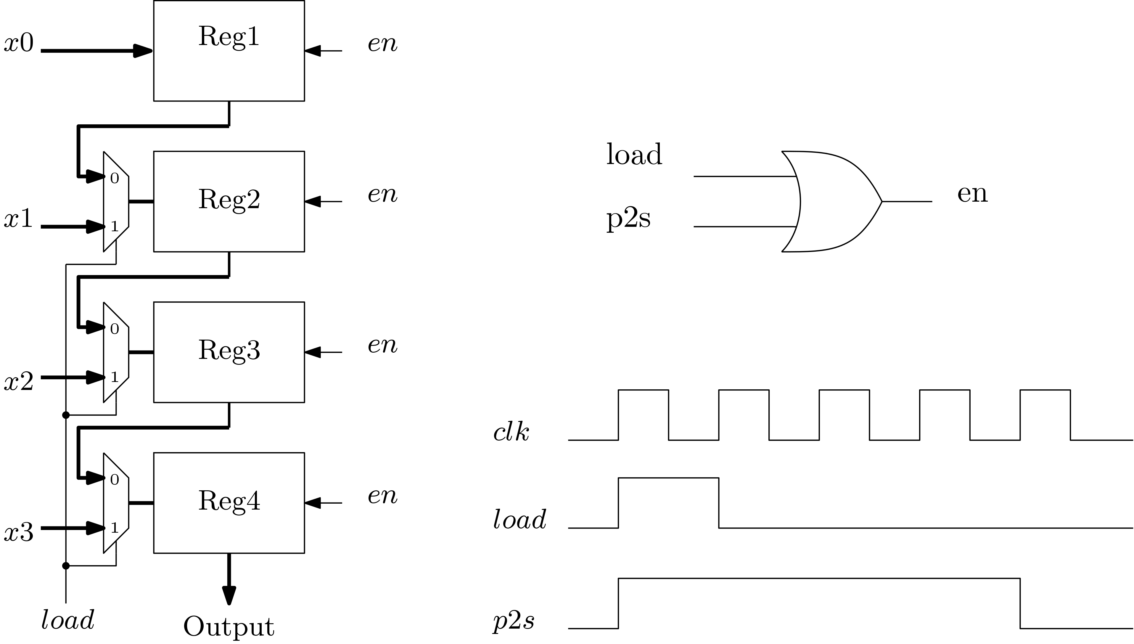
2. Serial to Parallel Conversion: The S2P block is shown in Fig. 4. for 4 data samples. This block has 4-registers of 16-bit width. Each register is controlled by a control enable pin. The input data flows to the output only when enable (en) signal is high. Timing diagram is also shown. The registers make the serial data into parallel in 4-clock cycles. For 8 data samples there will be 8-registers and it will take 8-clock cycles.

3. FFT Block: The FFT block is the main block which do the conversion of domain. The FFT block implements the signal flow diagram. We have structurally built the FFT block by the smaller sub-blocks. The architecture of the FFT block is shown in Fig. 5. We have applied moderate optimization to improve performance. The sub-blocks are discussed below.

A. Butter Fly Sub-Blocks: In the signal flow diagram in Fig. 1, the basic butterfly block does two type of basic operations, viz., addition and subtraction. Thus we have designed a basic Butter Block 1 (BF1) which performs addition and substraction. The Butter Fly block 2 (BF2) is actually a optimized version of two BF1 blocks which either zero real or imaginary part.

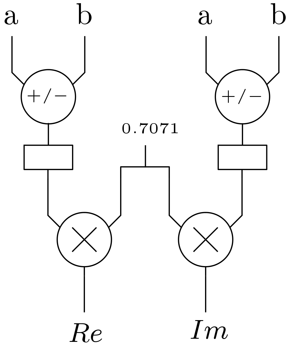
B. Complex Multiplier (CM): Complex multiplier multiplies two complex number. Multiplication of two complex number can be expressed as
![\[(a+jb)\times (c+jd) = ac+jad+jbc-bd = (ac-bd) + j(ad+bc)\]](https://digitalsystemdesign.in/wp-content/ql-cache/quicklatex.com-36d24178ef8cf1125c2b6b4a15d5d5cb_l3.png "Rendered by QuickLaTeX.com")
In our case, as  is variable but
  is constant. Thus the complex multiplication is reduced to the following.
![\[(a+jb)(0.7071 - j0.7071) = 0.7071(a+b) - j0.7071(a-b)\]](https://digitalsystemdesign.in/wp-content/ql-cache/quicklatex.com-172ad2b9b9f790749dd84504cf064375_l3.png "Rendered by QuickLaTeX.com")
![\[ (a+jb)(-0.7071 - j0.7071) = -0.7071(a-b) - j0.7071(a+b)\]](https://digitalsystemdesign.in/wp-content/ql-cache/quicklatex.com-8a5ed11c495bbd80d3fc42d991e3e4bb_l3.png "Rendered by QuickLaTeX.com")
The complex multiplier block is shown below in Fig. 7. The multiplication by 0.7071 is achieved by a constant multiplier. This reduces the hardware requirement.
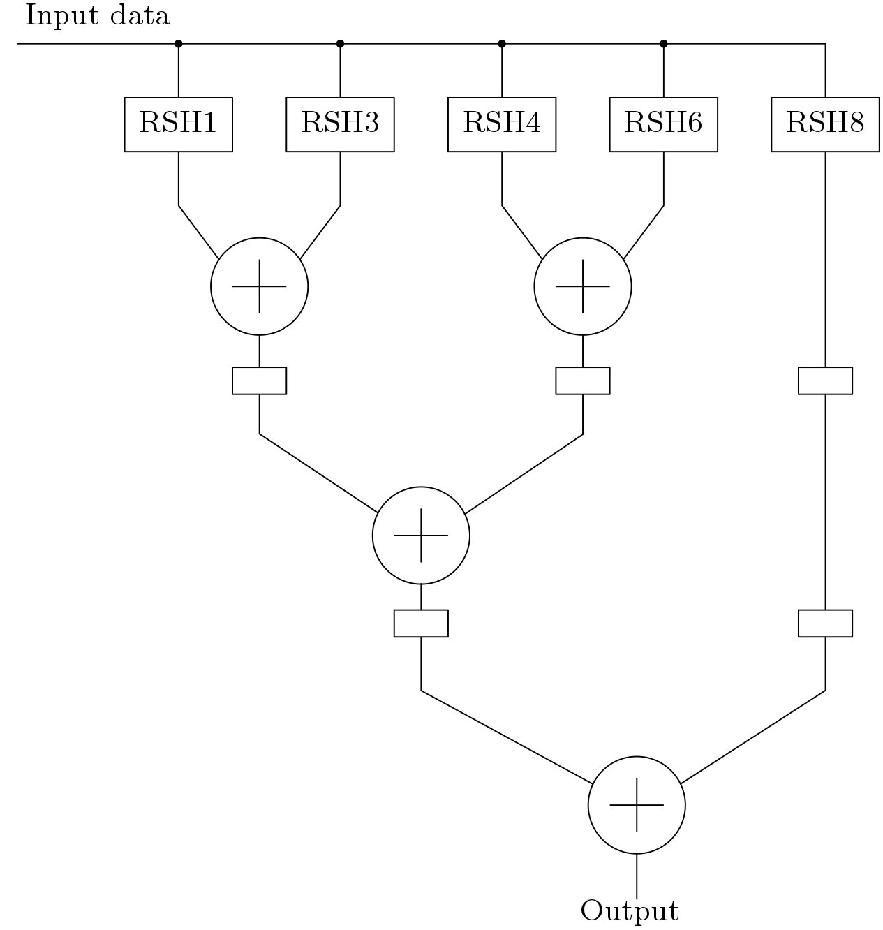
C. Constant Multiplier: The design of constant multiplier is discussed in detail in tutorials of computational circuits. The multiplication by the constant 0.7071 can be expressed as
![\[ 0.7071x = (2^{-1} + 2^{-3} + 2^{-4} + 2^{-6} + 2^{-8})x\]](https://digitalsystemdesign.in/wp-content/ql-cache/quicklatex.com-398fd17dcdb43733972369471947c169_l3.png "Rendered by QuickLaTeX.com")
The constant multiplier is shown in Fig. 8. The RSH blocks are hardware wire-shift blocks to shift in right direction.
D. Delay Block: The delay blocks are added to synchronize the operations. Several registers are connected serially to form delay blocks.
Further optimization is possible in the FFT block. Like, in the dotted box of Fig. 5 instead of 4 delay blocks two delay blocks can be placed before the SB2 block. This way applying optimization is necessary.
4. Parallel to Serial Conversion (P2S): After successful domain transfer by the FFT block, the parallel output from the FFT block must be made serial due output pin shortage or many systems accept serial data. The block diagram of P2S is shown in Fig. 9 for 4 data samples. The load pulse first loads the parallel data samples to the registers through the Muxes. Then the p2s signal made them serial. The timing diagram is also shown.
Control Path of The FFT Processor
Proper operation of the FFT processor needs proper design of the controller. The control path for the FFT processor is shown in Fig. 10. Two important blocks in designing the controller is
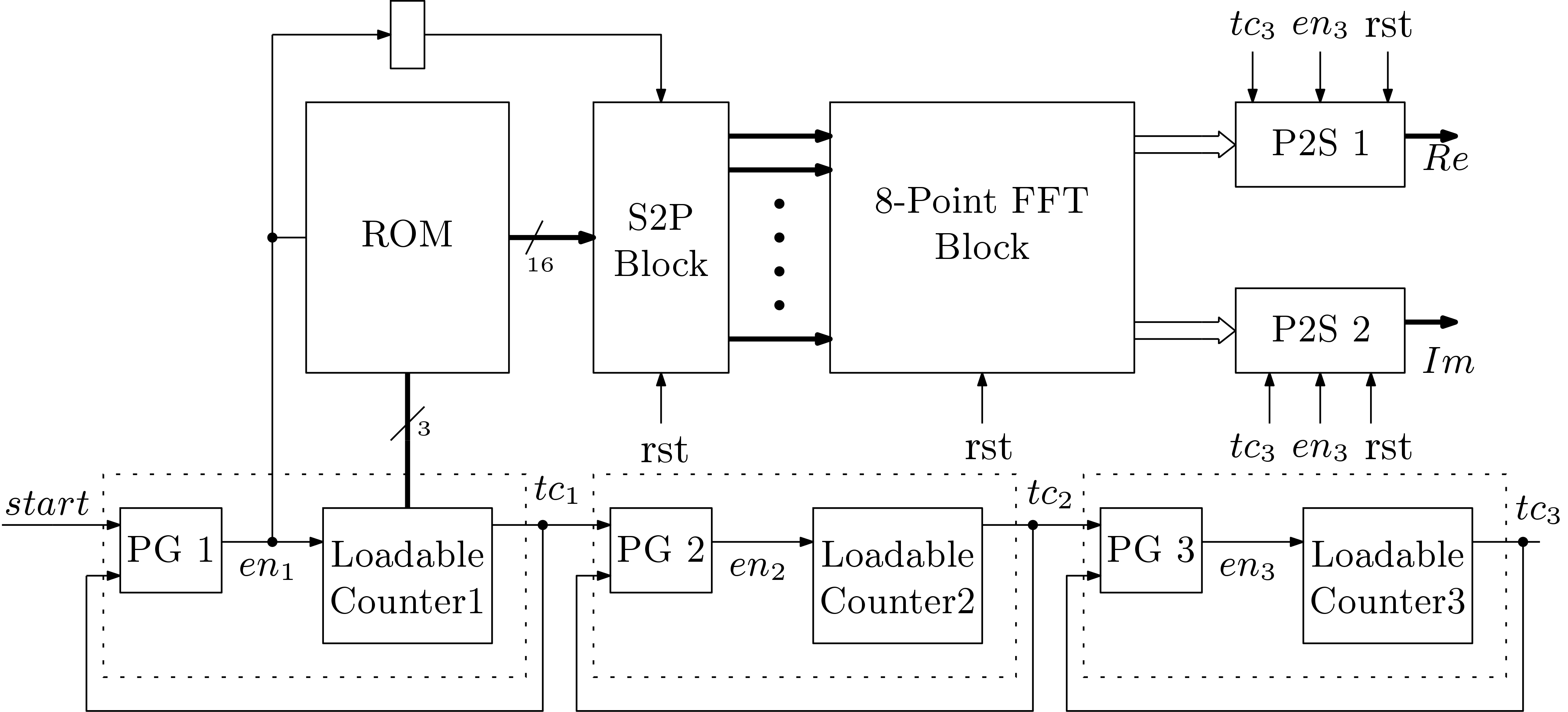
A. Phase Generation (PG) Block: The PG block is shown in Fig. 11. The output phase (q) is generated when a start pulse is given and q is deactivated when a stop pulse is asserted. This block can be generated in other way but we have shown a simpler way to realize this operation.

B. Loadable Counter: Loadable counters are discussed in the tutorials for sequential circuits. Loadable counter generate a Terminal Count (tc) signal when particular limit value (lmt) is reached.
The start pulse generates en1 signal which activates the ROM and also goes to S2P block for serial to parallel conversion. The counter 1 provides address to the ROM. The counter generates tc1 signal after 8 clock pulses. The tc1 signal triggers another PG block. The second set of PG and counter block is for tracking the latency of the FFT block. After the latency of the FFT block, tc2 signal is generated which again triggers the 3rd set of PG-Counter blocks. The tc2 and en3 signal works as load and p2s signals in P2S block respectively. The tc2 signal is synced with the first output of FFT block.
FFT Processor Output and Design Performance
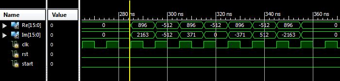
The output of the FFT processor is shown in Fig. 12 according to the example shown [1]. Input data samples are real but output is imaginary.
The FFT processor is implemented on SPARTAN 3E starter kit. The design performance is shown below in the following table.
| Parameters | FFT Implementation |
| FPGA Device | xc3s500e-4fg320 |
| Slice Register Count | 1030 (11%) |
| 4-Input LUTs Count | 831 (8%) |
| Occupied Slices Count | 777 (16%) |
| Maximum Frequency (MHz) | 229.51 |
| Dynamic Power (mW) | 329 |
Great article! We are linking to this great article on our site. Keep up the great writing.|
Please let me know if you’re looking for a article author for your site. You have some really great posts and I think I would be a good asset. If you ever want to take some of the load off, I’d love to write some articles for your blog in exchange for a link back to mine. Please blast me an email if interested. Many thanks!|
Hi there, just wanted to say, I enjoyed this article. It was helpful. Keep on posting!|
Thank you for sharing your knowledge.
Have you implemented this code on any fpga boards and got results?
If yes please help me in implementing this code on zedboard which I have.
I have been trying this for almost 6 months to implement.
I have implemented this code, but I have not got the results. I have used ILA9Integrated Logic Analyser) to capture results on laptop monitor.
let’s meet on any meeting plattform, and you guide me.
Yes…this code is implemented on FPGA. You can mention the problems you are facing while implementing the code.
Your means of describing all in this piece of writing is genuinely fastidious, every one be able to effortlessly understand
it, Thanks a lot.
Can you mention the architecture used in the design?
Is it Radix2² ?
please respond
It is the basic 8-point FFT architecture. I think its radix-2 not radix 2^2.
can u share the code to my email ,it would help for my case study
vj26869 @gmail.com
Don’t think that u are buying it.. Think that u are making a small contribution to the site….
Is this radix – 2^2 architecture?
I think it is simply radix -2 architecture not radix-2^2. You can refer any book for simple FFT signal flow for Decimation in Time.