In this tutorial, we will discuss FPGA implementation of a Median filter which is used for removing noises from an image. Noises in an image can be of various types like salt and pepper noise, Gaussian noise, periodic noise etc [1]. Out of these noises, salt and pepper noise is a very basic type of noise which can appear in any image. Salt and pepper noise can be easily characterized and removed in spatial domain.
Median Filter
Various type of spatial filters are proposed in literature to remove salt and pepper noise. Median filter is a very common and popular filter for image denoising. There are many variation of Median filter but here we will discuss the basic Median filter. The operating principle of a basic Median filter is based on replacing the pixel on which the window is operated by Median value of all the pixels inside that window. The image denoising using the Median filter for simple Grey scale image is shown in Figure 1.
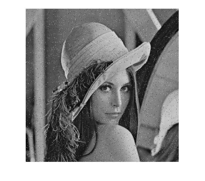
Figure 1(a): Noisy Image 
Figure 1(b): Filtered Image
In Grey scale image pixels values are ranging from  to
to  . Thus in a salt and pepper noise affected image, noisy pixel value can be either very close to 255 or as small as 0. The Median filter works based on the sliding window operation. A
  window can be set as
  ,
,  or
or  for an
  image and in a window their are
  pixels. The sliding window operation is shown in Figure 2 for a simple
  image. Here there are four rows of pixels. In the first step, Row 1 to Row 3 are operated and
  is the center pixel on which the window is operated. Then the window slides to the right and
  become the center pixel. Once the window slides to the extreme right then another Row takes part in the denoising operation. For example here in the second step, Row 2 to Row 4 are operated. Denoising operation can not be done on the boundary pixels.
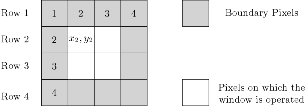 image.
FPGA Implementation of Median Filter
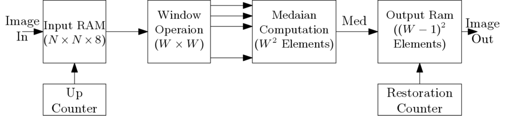
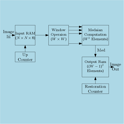
A simple architecture of the Median filter is shown in Figure 3. In FPGA implementation of median filter, there are three major steps which are Sliding window operation, Filtering operation and Filtered image restoration. The image acquisition is also an important operation which is achieved here by placing a dual port Input RAM of size  . A simple up counter is used here to write the pixels in the RAM block. Simultaneously the pixels can be read from the Input RAM block and fed to a block which does window operation. This block feds all the pixels in a window to the Median computation block. The Median value is then replaced in the original image in the restoration phase.
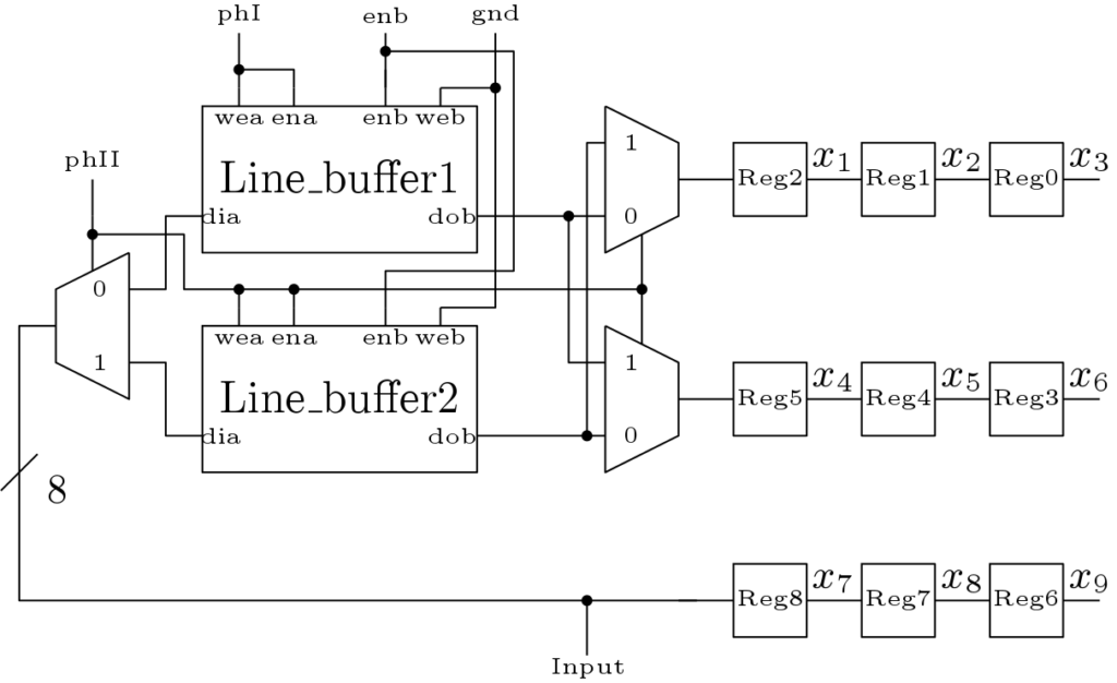
Here, window is chosen for image denoising. A simple scheme for sliding window operation reported in [2] is shown in Figure 4. Here, two line buffers are used and size of each is  . Initially, Row 1 is written to the Line buffer 1 through the DeMUX and in this time
  signal is high. Then Row 2 is written to the Line buffer 2 when the
  signal is high. The and signals are opposite and non-overlapping to each other. Now, Line buffer 1 has Row 1 and Line buffer 2 has Row 2. Row 3 is now read from the input RAM and at the same time both the buffers are also read. Simultaneously, Row 3 is also written to the Line buffer 1. Three clock cycles are needed to form the window using the nine registers.
 window operation.
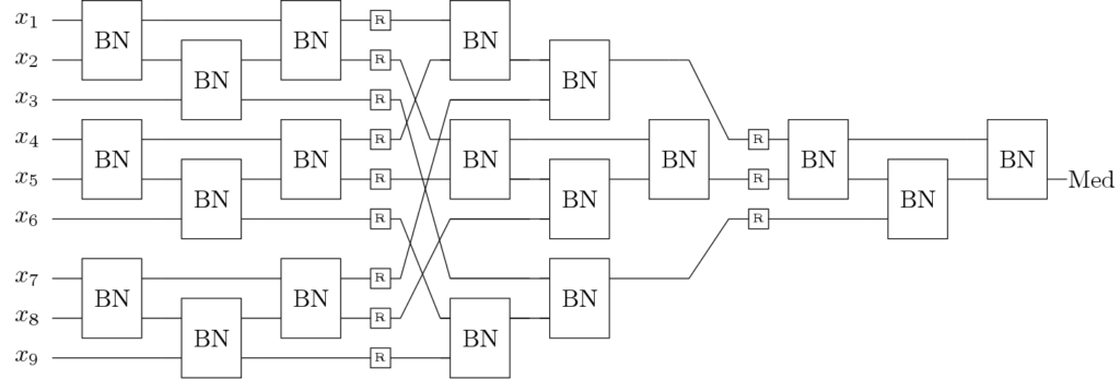
Various architectures are also reported to find Median efficiently. The Median computation block reported in [3] is adopted here and is shown in Figure 5. This parallel architecture uses total 19 BN blocks. The structure of the BN block is already discussed in the previous tutorial for sorting. Here, pipeline registers are inserted to improve the timing performance. It is certain that increasing the value of  will increase the number of BN blocks.
In the image restoration phase, noisy pixels are replaced with the corrected one. This restoration can be done on the input image also. But here a separate output RAM is used. Note that in order to retain the boundary pixels, the output RAM should initially contain the boundary pixels. A restoration counter write the Median values in the output RAM at their exact location. If the size of the image is  then the restoration counter will count as

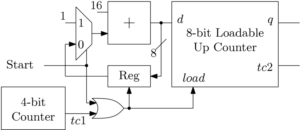
A possible scheme of the restoration counter is shown in the Figure 6. Two loadable counters are used, one is of 8-bit and another is of 4-bit. The 4-bit counter is used to load the 8-bit counter with the load values  as
as  . Initially the
  signal loads the 8-bit counter with
  . Then both the counter starts counting. The 4-bit counter counts upto
  and generate
  signal which again loads the 8-bit counter with next load value. Both the counters have a common enable input. This way the restoration counter works.
References
- R.C.Gonzalez and R. Woods, Digital Image Processing. Prentice Hall,
2007. - P.-Y. Chen, C.-Y. Lien, and H.-M. Chuang, “A low-cost vlsi implementation for efficient removal of impulse noise,” Very Large Scale Integration (VLSI) Systems, IEEE Transactions on, vol. 18, no. 3, pp. 473–481, 2010.
- J.L.Smith, “Implementing median filters in xc4000e fpgas,” in Proc. of VII, 1996, p. 16.
Verilog Code of Median Filter for Denoising
There are many filter techniques in literature to remove noise from an image. Among them median filter is simple but have acceptable performance in removing salt and pepper noise. Here, a Verilog code is provided to implement median filter on FPGA along with Matlab codes.