Automatic Test Pattern Generation and Automatic Test Pattern Generator (ATPG) is an electronic design automation method/technology used to find an input (or test) sequence that, when applied to a digital circuit, enables automatic test equipment to distinguish between the correct circuit behavior and the faulty circuit behavior caused by defects. Earlier we presented a tutorial on ATPG for Combinational Circuits. This tutorial focuses on ATPG for sequential circuits using Synopsys Tetramax tool.
1. Open the terminal
2. Source the synopsys.cshrc
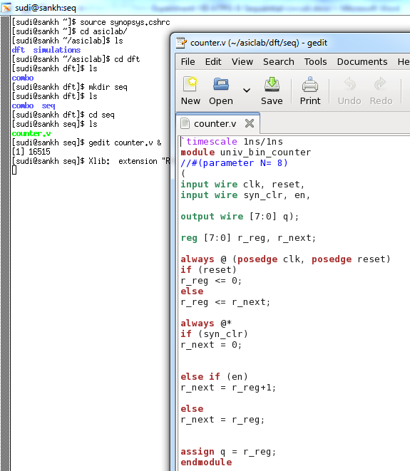
3. In a ASIC lab directory, make design.v (any sequential circuit). In this experiment, we perform ATPG for Sequential circuits. In our previous experiment we have performed ATPG for combinational circuits. Scan insertion is not required for combinational circuits, but it is required for sequential circuits. Scan insertion can be done in DFT compiler which is a integral part of design vision.
4. Open the design vision and execute the following commands. We generate scan inserted synthesized netlist at the end. We also extract spf (STIL procedure file) , which is a input to the Tetramax used for ATPG. (Note: STIL: – Standard Test Interface Language).
5. Make your design ready.
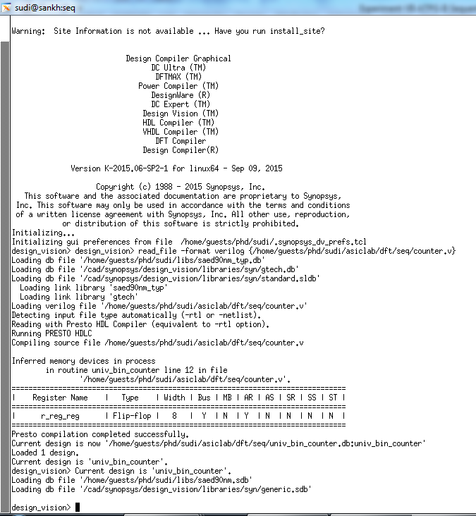
6. Open design_vision. Read the library and design into design vision.

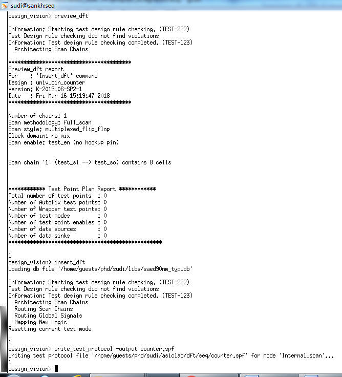
7. Go the terminal as below and execute the following commands to insert dft (scan chain) and spf file.
8. Execute the following commands :-
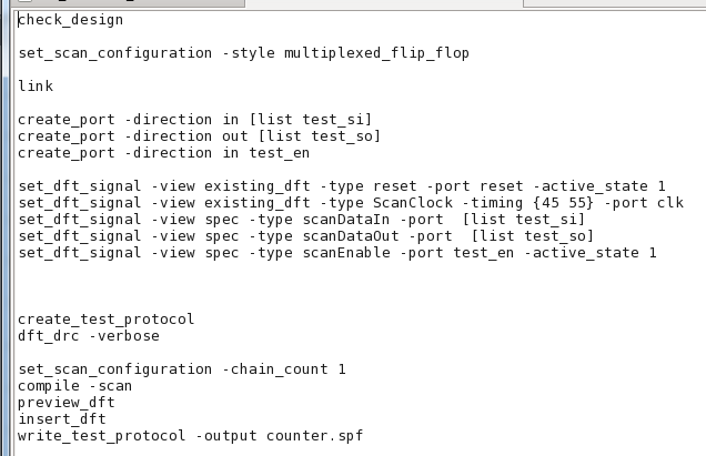
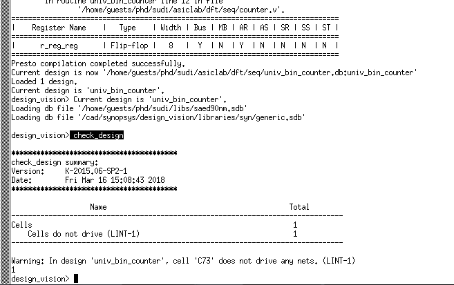
9. Execute all DFT related commands as below: –
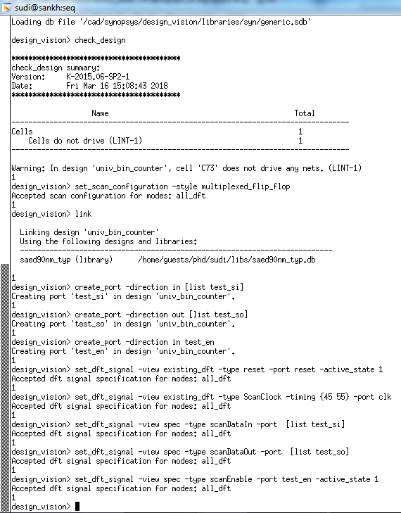
10. Continue :-
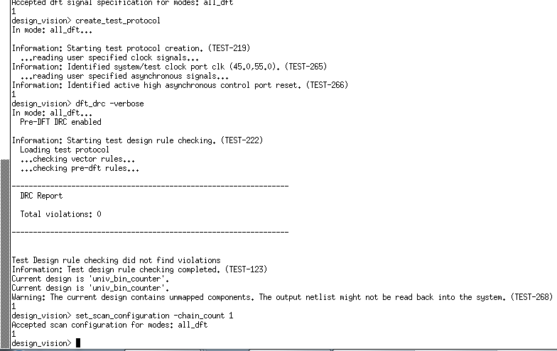
11. Continue :-

12. Continue :-
13. Save the scan inserted netlist as below: –
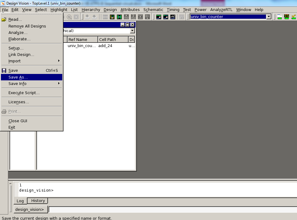
14. Continue: –
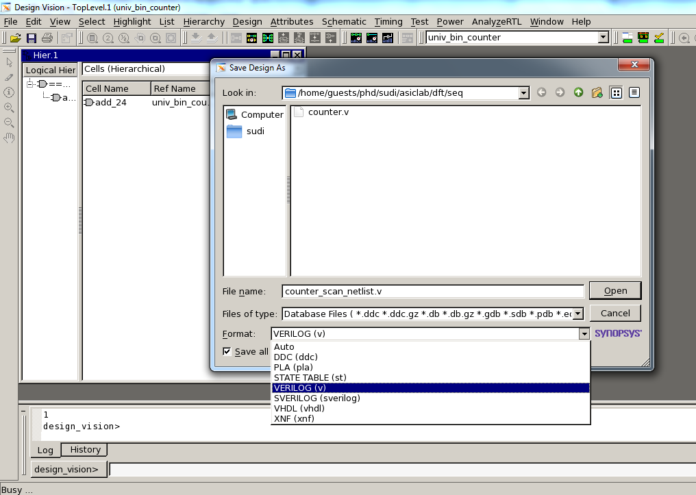
15. File- Exit- Design _Vision.
16. Open the counter_scan_netlist.v and observe the difference between your earlier counter_net.v and scan inserted counter_scan_netlist.v
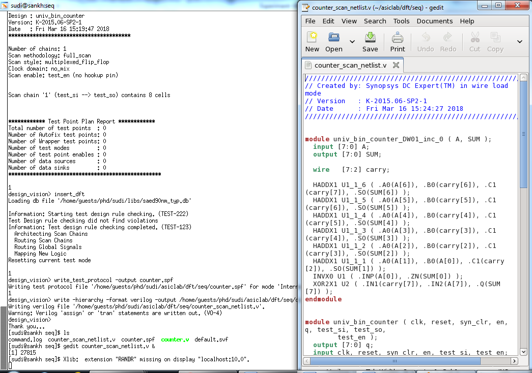
18. Open the Tetramax and generate ATPG

18. Simulate the ATPG using VCS as before.
Post Credit

Faculty Advisor: Prof. Kamalakanta Mahapatra
Instructor: K Sudeendra, Teaching Assistants: S K Ram, J P Mohanty
VLSI Laboratory
The VLSI laboratory at ECE Department of NIT Rourkela is obliged towards the support and encouragement of Ministry of Electronics and Information Technology, Government of India. The overall activities is purely supported by the Special Manpower Development Program for Chips to System Design (SMDP-C2SD) project.
