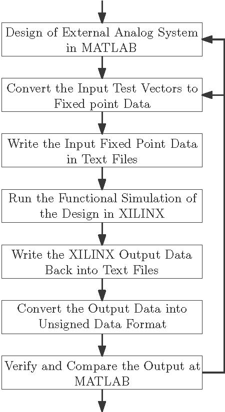
Design verification is must in designing any system. Design verification and testing is the most tedious job in implementing any complex system. Several foundries are specialized in doing verification and testing. Each and every step of VLSI design needs verification. If there is a fault in any step, one has to go to the early steps to correct it. There are two types of verifications generally carried out in making VLSI design. They are
- Functional verification
- Static Timing Analysis
The functional verification step verifies the functionality of the design or the behavior of the system. On the other hand static timing analysis (STA), concentrates on verifying the timing constraints. Both the verification steps must be carried out after every step such as translation, placing and routing.
In this post, functional verification of FPGA implementations is discussed. Smaller designs can be verified by writing test benches. But it is very difficult to verify the complex designs. Also, if the design involves several memory elements it is very difficult to create such huge amount of memory locations. Designers face difficulties in loading test vectors in memory elements several times. In this post, a simple way of design verification is discussed.
Functional Verification Approaches
Functional verification of design can be carried out using two methods in general and they are
- MATLAB/Any similar tool based.
- XILINX/Any similar tool based.
MATLAB based Verification: MATLAB provides a very easy system verification platform as both the analog and

Figure 1 :Functional verification using MATLAB
MATLAB based verification provides an easy solution to the design verification. Most of the VLSI designers avoid this kind of verification as there are few scopes where a designer can improve the design. For an expert designer, who seeks to improve the performance of the design must do design and verification at
XILINX based Verification
XILINX also provides an easy way of functional verification. If a designer is designing a system in XILINX, then the designer need not import all the HDL codes to MATLAB. The general scheme for verification is shown below

Figure 2: XILINX based functional verification.
The XILINX based system verification can be explained by an example. Consider, a designer has to solve the linear equation y = ax, where y is an output vector, a is a square matrix and x is the input. The problem is to find the x by the equation x = inv(a)y. To do that designer is supposed to find the inverse of a and multiply with y in FPGA.
To begin with this simple problem, the output y can be generated in MATLAB or y may be the output of an external analog system. The digital part of the system takes y and matrix a as inputs and produces x as output. Consider that the matrix a is constant and need to be stored in memory inside FPGA. So the only varying input is y. If y is generated through MATLAB then the interface between a COMPUTER and FPGA can done by serial UART protocol or using LAN or using SPI flash technique. If y is the output of an external system then the analog system can interfaced with FPGA using interfacing ADC with the FPGA. After interfacing, FPGA processes and produces the output x. The output x can be seen back in the MATLAB using same interface mechanisms mentioned above or it can be seen in a CRO screen using interfacing a DAC with the FPGA.
Following discussion focuses on designing the analog part in MATLAB and importing the FPGA output back into MATLAB for comparison. The input vector y is generated in MATLAB and stored in a XLSX file. The input vector y is converted to

We have considered handling of XLSX files using MATLAB. The codes are described and attached below.
Reading from a text file.
The command fopen() opens a file input_vector.txt in read mode. In the loop of j, jth element of input_vector.txt (of0) stored in register A1. Then the content of A1 is stored in jth location of b which is an array of registers.
module mem_read(C1,ada,clk);
    input [9:0] ada;
	 input clk;
    integer of0;
    output reg [17:0] C1;
    reg [17:0] A1;
	 reg [17:0] b1 [1023:0];
	 integer j;
	 initial begin
	 of0=$fopen("input_vector.txt","r");
	 for (j=0;j<=1023;j=j+1)
	 begin
        $fscanf(of0,"%d\n",A1);
         #1;
        b1[j] = A1;
    end
	 $fclose(of0);
	 end
    always @ (posedge clk)
    begin
	 C1 = b1[ada];
	 end
endmodule
Writing into a text file.
The value of the register A is written in the file output_vector.txt only if en is high and with positive edge of clock. The clock is considered to be of period 10 ns.
module mem_write(A,en,clk);
    integer of0;
    input [17:0] A ;
	 input en,clk;
	 integer j;
	 initial begin j = 0; end
	 always @(posedge clk)
	 begin
	 if (en)
	      begin
	 of0=$fopen("output_vector.txt","w");
	   for (j=0;j<=4;j=j+1)
  	      begin
	 $fdisplay(of0,"%d\n",A);
	 #10;
	      end
		   end
	 else
	 $fclose(of0);
	 end
endmodule
The MATLAB codes are not discussed here. They are attached with the post.
