Contents for combinational circuits are
- Addition/Subtraction
- Controlled Add_sub
- Decoder
- Converters
- Parity Check and Generator
- Comparator Design
- Wired Shift
- Variable Shift Block
- Scale Block
Combinational Circuits
In this post, the realization of various basic combinational circuits using Verilog is discussed. There is no need to discuss the theory behind the combinational blocks. More about the theoretical concepts can be found in any digital electronics book. Though some of the important blocks are discussed in detail and for others only the Verilog code is given in this post.
Half Adder
module ha(

  input a,b,

  output sum,co

    );

assign sum = a^b;

assign co = a&b;

endmodule
Full Adder using Half Adder
module fa(a,b,cin,sum,co);

input a,b,cin;

output sum,co;

wire t1,t2,t3;

ha X1(a,b,t1,t2);

ha X2(cin,t1,sum,t3);

assign co = t2 | t3;

endmodule
Full Subtractor
module Subtractor(

  input a,b,bin,

  output d,bout

    );

wire a_bar;

assign a_bar = ~a;

assign d = a^b^bin;

assign bout = (b&bin)|(b&a_bar)|(a_bar&bin);

endmodule
Ripple Carry Adder
module RCA(a,b,cin,sum,co);

input [3:0] a,b;

input cin;

output [3:0] sum;

output co;

wire c1,c2,c3;

fa m1(a[0],b[0],cin,sum[0],c1);

fa m2(a[1],b[1],c1,sum[1],c2);

fa m3(a[2],b[2],c2,sum[2],c3);

fa m4(a[3],b[3],c3,sum[3],co);

endmodule
Controlled Adder/Subtractor
Controlled adder/subtractor block is one of the most important combinational circuits in designing digital systems. Addition and subtraction operation is performed by the same logic block using two’s complement arithmetic. The block diagram is shown below for data width 4-bit. When the ctrl input is high, subtraction is performed and when the ctrl is low, the addition operation is performed.
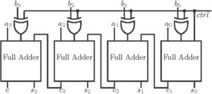
Control Adder/subtractor
module Add_sub(a,b,ctrl,s,c);

input [3:0] a,b;

input ctrl;

output [3:0] s;

wire [3:0] b1;

output c;

wire c1,c2,c3;

assign b1[0] = ctrl ^ b[0];

assign b1[1] = ctrl ^ b[1];

assign b1[2] = ctrl ^ b[2];

assign b1[3] = ctrl ^ b[3];

fa m1(a[0],b1[0],ctrl,s[0],c1);

fa m2(a[1],b1[1],c1,s[1],c2);

fa m3(a[2],b1[2],c2,s[2],c3);

fa m4(a[3],b1[3],c3,s[3],c);

endmodule
Decoder/Encoder/Priority Encoder
A Verilog code for 3 to 8 decoder is shown below. Similarly, Encoder or priority Encoder can be realized.
module decoder3_8(

   input [2:0] s,

   output [7:0] z

    );

reg [7:0] z;

always @ (s)

case(s)

3'b000 : z = 8'b10000000;

3'b001 : z = 8'b01000000;

3'b010 : z = 8'b00100000;

3'b011 : z = 8'b00010000;

3'b100 : z = 8'b00001000;

3'b101 : z = 8'b00000100;

3'b110 : z = 8'b00000010;

3'b111 : z = 8'b00000001;

default : z = 8'b0000000;

endcase

endmodule
BCD to Binary Converter
module BCD2BIN(

   input [7:0] bcd,

   output [7:0] bin

    );

wire [3:0] t1,t2,t3,t4,sum1,sum2;

wire co1,co2;

parameter cin = 1'b0;

assign t1 = {bcd[5],bcd[3],bcd[2],bcd[1]};

assign t2 = {1'b0,bcd[4],bcd[5],bcd[4]};

RCA m1(t1,t2,cin,sum1,co1);////4-bit ripple carry adder

assign t3 = {1'b0,co1,sum1[3],sum1[2]};

assign t4 = {bcd[7],bcd[6],bcd[7],bcd[6]};

RCA m2(t3,t4,cin,sum2,co2);////4-bit ripple carry adder

assign bin = {co2,sum2,sum1[1:0],bcd[0]};

endmodule
Binary2Grey and Grey2Binary conversion
module B2G(

   input [3:0] b,

   output [3:0] g

    );

assign g[0] = b[0] ^ b[1];

assign g[1] = b[1] ^ b[2];

assign g[2] = b[2] ^ b[3];

assign g[3] = b[3];

endmodule

module G2B(

   input [3:0] g,

   output [3:0] b

    );

assign b[0] = g[0] ^ b[1];

assign b[1] = g[1] ^ b[2];

assign b[0] = g[2] ^ b[3];

assign b[0] = g[3];

endmodule
Parity Checker and Generator
Parity check and generation is an error detection technique in digital transmission of bits. A parity bit is added to the data to make the number of 1s either even or odd. In even parity bit scheme, the parity bit is ‘0’ if there are even number of 1s in the data and the parity bit is ‘1’ if there are odd number of 1s in the data. In odd parity bit scheme, the parity bit is ‘1’ if there are even number of 1s in the data and the parity bit is ‘0’ if there are odd number of 1s in the data. Parity bit is generally added in the MSB.
Realization of both type of parity for 4-bit data is described below. If evn_parity is ‘1’ then there are odd number of 1’s in the data.
module paritycheck_generate(

   input [3:0] a,

   output [4:0] odd_out,evn_out

    );

wire evn_parity,odd_parity;

///Parity Check

assign evn_parity = (a[0]^a[1]^a[2]^a[3]);

assign odd_parity = ~evn_parity;

////generate parity.....for ODD parity

assign {odd_out[4],odd_out[3:0]} = {odd_parity,a[3:0]};

////generate parity.....for EVEN parity

assign {evn_out[4],evn_out[3:0]} = {evn_parity,a[3:0]};

endmodule
Comparator Design
In this tutorial, the design of a comparator is explained in detail. A 16-bit comparator is designed in the behavioral style of modeling and also in the structural style of modeling.
Behavioral style
In behavioral style, a comparator can be designed by knowing only the output characteristics of a comparator. Hence it is very simple to design comparators of any data width without knowing the logic inside.
module comp_beh(a,b,lt1,eq1,gt1);

input [15:0] a,b;

output reg lt1,eq1,gt1;

always @(a or b)

begin

lt1=0; eq1=0; gt1=0;

if(a==b)

eq1=1;

else if (a>b)

gt1=1;

else

lt1=1;

end

endmodule
Structural Design
Though it is very simple to design a comparator in behavioral style, a VLSI circuit designer should have the knowledge of the internal logic of a comparator. In this tutorial, a 16-bit comparator is realized by the most basic block which is a 1-bit comparator.
Comparator (1-bit):-
The logic diagram of a 1-bit comparator is shown below. It is an optimized logic block. Equality condition of two bits can be checked by the basic Ex-NOR gate. Here in place of EX-NOR, a NOR gate is used after optimization.
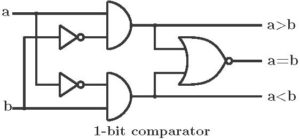
module comp_1bit(a,b,lt,eq,gt);

    input a,b;

    output lt,gt,eq;

     wire abar,bbar;

assign abar = ~a;

assign bbar = ~b;

assign lt = abar & b;

assign gt = bbar & a;

assign eq = ~(lt|gt);

endmodule
Comparator (4-bit)
The 4-bit comparator block is designed by the basic 1-bit comparator. Total four 1-bit comparators are used. 4-bit comparator block is designed as a more general block. It has four control input lines gt1, lt1 and eq1 to support cascading with other 4-bit comparators.
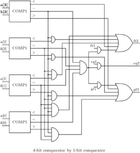
The Verilog code the 4-bit comparator is shown below.
module comp4(A,B,LT1,GT1,EQ1,LT2,GT2,EQ2);

    input [3:0] A,B;

    output LT2,GT2,EQ2;

    input LT1,GT1,EQ1;

wire x30,x31,x32,x20,x21,x22,x10,x11,x12,x00,x01,x02;

wire x40,x41,x42,x50,x51,x52,x61,x62;

comp_1bit  c3(A[3],B[3],x30,x31,x32);

comp_1bit  c2(A[2],B[2],x20,x21,x22);

comp_1bit  c1(A[1],B[1],x10,x11,x12);

comp_1bit  c0(A[0],B[0],x00,x01,x02);

assign x40 = x31 & x20;

assign x41 = x31 & x21 & x10;

assign x42 = x31 & x21 & x11 & x00;

assign x50 = x31 & x22;

assign x51 = x31 & x21 & x12;

assign x52 = x31 & x21 & x11 & x02;

assign EQ = (x31 & x21 & x11 & x01);

assign EQ2 = EQ & EQ1;

assign x61 = EQ & LT1;

assign x62 = EQ & GT1;

assign LT2 = (x30 | x40 | x41 | x42) | x61;

assign GT2 = (x32 | x50 | x51 | x52) | x62;

endmodule
Comparator (16-bit)
A 16-bit comparator is realized using 4-bit comparator. Total four comparators are used. As mentioned previously that 4-bit Comparator block is designed as a general block. The inputs lt1, gt1, eq1 are given to the first 4-bit comparator which compares the lower 4-bits. The eq1 input should be equal to ‘1’ to enable comparison and the other two inputs are must be ‘0’. Likewise, Comparator for higher bit-lengths can be designed.
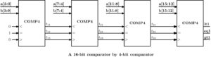
The Verilog code for the 16-bit Comparator is shown below.
module comp16(a,b,lt1,gt1,eq1);

input [15:0] a,b;

output lt1,gt1,eq1;

parameter eq =1'b1;

parameter lt=1'b0;

parameter gt=1'b0;

wire t11,t12,t13,t21,t22,t23,t31,t32,t33;

comp4 c1(a[3:0],b[3:0],lt,gt,eq,t11,t12,t13);

comp4 c2(a[7:4],b[7:4],t11,t12,t13,t21,t22,t23);

comp4 c3(a[11:8],b[11:8],t21,t22,t23,t31,t32,t33);

comp4 c4(a[15:12],b[15:12],t31,t32,t33,lt1,gt1,eq1);

endmodule
Division/Multiplication by Constant Number
Wired Shifting
Hardware complexity for multiplication operation is higher than that of addition or subtractor blocks. Signed multipliers are even more critical. To multiply/divide a number by power of 2, a multiplier/divider block is not required. It can be achieved in a much simpler way. For multiplication, bits are left shifted and for the division, bits are right shifted. The shifting of bits is achieved by a simple combinational circuit which is shown below.
Example:
- a = 0101, after multiplication by 2 result is1010.
- a = 0110, after division by 2 result is 0011.
An easy approach to achieve this is shown below for signed data in 2’s complement representation.
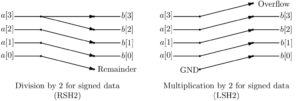
In Verilog, this can be achieved by concatenation.
module rsh1(a,b);

    input [3:0] a;

    output [3:0] b;

assign {b[3:2],b[1:0]}= {a[3],a[3],a[2:1]};

endmodule
This kind of block is named as RSH1 for division by 2 or shifting of 1-bit right.
Controlled Shift Block
The controlled shift block is described below. When the input signal ‘s’ is high, input data is shifted to perform division by 2. Otherwise, input data is passed unaffected to the output.
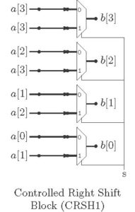
The CRSH1 block in Verilog is realized as.
module CRSH1(a,b,s);

input [3:0] a;

output [3:0] b;

input s;

mux_df m1(a[3],a[3],s,b[3]);

mux_df m2(a[2],a[3],s,b[2]);

mux_df m3(a[1],a[2],s,b[1]);

mux_df m4(a[0],a[1],s,b[0]);

endmodule
Variable Shift Block
Same block can be used to achieve variable shifting. The Variable Right Shift Block (VRSH) is shown below for data width 18.
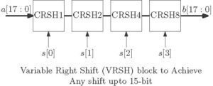
When control input data s = 4’b0000, input ‘a’ is passed to the output as it is. For example, when the input s = 4’b1010, the blocks CRSH2 and CRSH8 are active. So the input will be shifted by 10 –bit.
The Verilog code for this block is shown below.
module VRSH_18(a,b,s);

input [17:0] a;

output [17:0]b;

input [3:0] s;

wire [17:0] t1,t2,t3;

CRSH1_18 m1(a,t1,s[0]);

CRSH2_18 m2(t1,t2,s[1]);

CRSH4_18 m3(t2,t3,s[2]);

CRSH8_18 m4(t3,b,s[3]);

endmodule
The Verilog codes for the sub-modules are shown in the Verilog file attached below or can be found in the download section.
Scale Block – Constant Multiplier
This block is one of the most important combinational circuits, used in designing digital systems. To multiply by a constant data, complex multiplier blocks are not used. Instead, a scale block is used to approximate the result.
For example, to divide an input data stream by a constant value 3, a divider block should not be used. Division by 3 is equivalent to the multiplication by 0.3333 which can be expressed approximately as

The scale block to divide an input data ‘a’ by a constant value 3 is shown for 18-bit data width with 9 bit for the fraction. The input data is right shifted by 2-bit, 4-bit, 6-bit and 8-bit. The results after each shifting function are added to produce the final result. The accuracy depends on the number of bits used to represent the fraction part in fixed-point data format.
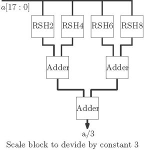
RSH2, RSH4, RSH6 and RSH8 blocks are mentioned earlier in the tutorial. As an example when input data 6 is divided by 3 by the scale block, result is 1.992 in 18-bit word length. The Verilog code for the scale block to divide by a constant value 3 is shown below.
module scale3(a,b);

input [17:0] a;

output [17:0] b;

wire [17:0] t1,t2,t3,t4,t5,t6;

wire co1,co2,co3;

parameter cin = 1'b0;

rsh2 m1(a,t1);

rsh4 m2(a,t2);

rsh6 m3(a,t3);

rsh8 m4(a,t4);

adder_18 m5(t1,t2,cin,t5,co1);

adder_18 m6(t3,t4,cin,t6,co2);

adder_18 m7(t5,t6,cin,b,co3);

endodule
The Verilog codes for the sub-modules are shown in the Verilog file attached below or can be found in the download section.
Click here to download the file.
This website is very useful. one should go through this once
Thank you for visiting…….
for each style of design in Verilog there will be pro’s and con’s(ex. no.of blocks occupied, delay etc.) could you highlight them.
See, advantage of behavioral style is that u can design easily. But optimization is very difficult and for some cases it is not possible.
Structural style is similar to custom design approach. Time taking but fruitful in the end.
For basic blocks we can use any kind of style. But for integration structural modelling must be used.
great explanation.
Thank you Santra…Keep following my blogs…….
I do not even know how I finished up here, however I believed this put up used to be great. I don’t know who you might be but certainly you’re going to a famous blogger in the event you aren’t already 😉 Cheers!
Thanks for visiting. I think you will help me to promote this blog.
whoah this blog is excellent i love reading your articles. Keep up the great work! You know, many people are looking around for this information, you could help them greatly.
Yaah…..that is why the blog is created. I hope contents are actually interesting to you.
Its like you read my mind! You appear to know so much about this, like you wrote the book in it or something.
I think that you could do with some pics to drive
the message home a little bit, but other than that,
this is magnificent blog. A fantastic read.
I will certainly be back.